


 It’s Only Common Sense: If You’re Not Differentiated, You’re Dead
 Alpha Insights, Performance by Design: The Future of PCB Manufacturing in the Midwest
 Happy’s Tech Talk #43: Engineering Statistics Training With Free Software


Not All Plating Lines Are Created Equal
February 12, 2020 | I-Connect007 Editorial TeamEstimated reading time: 12 minutes
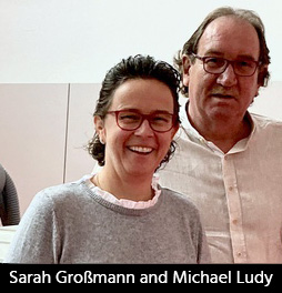
Barry Matties and Happy Holden met with CEO Michael Ludy and CMO Sarah Großmann from Ludy, a company specializing in galvanic plating equipment for PCBs. During one of I-Connect007’s visit to GreenSource Fabrication, the team found Ludy equipment being utilized there, so Barry and Happy traveled to their factory in Germany to learn more about the company.
The following interview gives an overview of Ludy and their latest advancements in PCB plating equipment.
Barry Matties: Let’s start with a little bit about your product.
Sarah Großmann: We produce galvanic plants for PCBs. That’s our main task. We have a highly specialized way of having the galvanic tanks and the geometry of the tanks, where the plating and the aspect ratio is much better. We tried to focus mainly on PCBs in the past years. We fulfilled the demands and ideas of Alex Stepinski and what he thought could work. We are flexible and gave him a plant with the newest technology. He can fulfill his plating demands and multiple processes internally.
Generally, this is the main thing we do, but we also do the research for waste-air-free and wastewater-free galvanic plants like the GalvanoMat® PCB. That’s our main idea of fulfilling a complete green fabrication in one. You have one container where the galvanic plant is inside, and one container getting the waste air, wastewater, and energy recovery, and everything goes in one circle. You don’t have to waste that much and fulfill all the green fabrication requirements that are needed.
We have it for metal finishing and PCBs. We’re trying to get back in the U.S. market. We were there already. The lines are still running, and it’s going more and more to green fabrication. This is why we mostly do R&D for the GalvanoMat® PCB.
Figure 1: Overview of the latest generation of Ludy plating line with split-tank hoist access.
Happy Holden: People would probably buy brand new plating equipment because of high-density interconnect (HDI) and substrate-like PCBs (SLPs). All of which have very tiny holes and a much higher aspect ratio, which the conventional anode to cathode and one-axis agitation or area agitation is not sufficient for the throwing power and things like that.
Großmann: The anodes are inside, and every one of those segmented anodes is separately controlled by a rectifier.
Holden: Can you do pulse plating too?
Großmann: It would be possible, depending on the chemistry. The problem is that in the galvanic plant area, the people stick to what they know and don’t want to invest high amounts of money for testing around. This is a problem. That’s why the research steps are not very fast compared to other machine areas. They know that the chemistry is also influencing this area, and if Atotech says they’re not sure, then nobody will invest money on that. That’s why we are pretty happy that our solution worked and was inclusive with a 3D agitation drive. We have a very good distribution overall of the PCB on both sides. Those are the main benefits of the system.
Holden: The North American market has the common board, but then they have leading-edge things for medical, aerospace, or radar, where they want to go to a much higher aspect ratio both on through-holes and on blind vias. The problem is typical galvanic equipment isn’t there yet. Some believe the Ludy equipment will take them there, which means adopting the old way. There’s a big difference in productivity between four hours and 50 minutes.Page 1 of 4
Share on:


Testimonial
"Our marketing partnership with I-Connect007 is already delivering. Just a day after our press release went live, we received a direct inquiry about our updated products!"
Rachael Temple - AlltematedSuggested Items
Nolan’s Notes: Tariffs, Technologies, and Optimization
10/01/2025 | Nolan Johnson -- Column: Nolan's NotesLast month, SMT007 Magazine spotlighted India, and boy, did we pick a good time to do so. Tariff and trade news involving India was breaking like a storm surge. The U.S. tariffs shifted India from one of the most favorable trade agreements to the least favorable. Electronics continue to be exempt for the time being, but lest you think that we’re free and clear because we manufacture electronics, steel and aluminum are specifically called out at the 50% tariff levels.
MacDermid Alpha & Graphic PLC Lead UK’s First Horizontal Electroless Copper Installation
09/30/2025 | MacDermid Alpha & Graphic PLCMacDermid Alpha Electronics Solutions, a leading supplier of integrated materials and chemistries to the electronics industry, is proud to support Graphic PLC, a Somacis company, with the installation of the first horizontal electroless copper metallization process in the UK.
Electrodeposited Copper Foils Market to Grow by $11.7 Billion Over 2025-2032
09/18/2025 | Globe NewswireThe global electrodeposited copper foils market is poised for dynamic growth, driven by the rising adoption in advanced electronics and renewable energy storage solutions.
MacDermid Alpha Showcases Advanced Interconnect Solutions at PCIM Asia 2025
09/18/2025 | MacDermid Alpha Electronics SolutionsMacDermid Alpha Electronic Solutions, a global leader in materials for power electronics and semiconductor assembly, will showcase its latest interconnect innovations in electronic interconnect materials at PCIM Asia 2025, held from September 24 to 26 at the Shanghai New International Expo Centre, Booth N5-E30
Trouble in Your Tank: Implementing Direct Metallization in Advanced Substrate Packaging
09/15/2025 | Michael Carano -- Column: Trouble in Your TankDirect metallization systems based on conductive graphite are gaining popularity throughout the world. The environmental and productivity gains achievable with this process are outstanding. Direct metallization reduces the costs of compliance, waste treatment, and legal issues related to chemical exposure. A graphite-based direct plate system has been devised to address these needs.