


 Dan’s Biz Bookshelf: Four Important Books You Need to Read (Not Just Say You Have)
 Marcy’s Musings: Advancing the Advanced Materials Discussion
 The Marketing Minute: Cracking the Code of Technical Marketing


Isola Opens Expanded R&D and Analytical Laboratory in Arizona
June 19, 2020 | PR NewswireEstimated reading time: 2 minutes
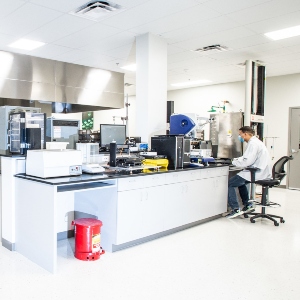
Isola, designer and developer of copper-clad laminates and fabrication materials for multi-layer printed circuit boards (PCBs), has officially opened an expansive R&D and analytical services laboratory at the company's new global headquarters in Chandler, Ariz.
Nearly doubling the size and capacity of the testing facility enables enhanced product development, material qualification, application engineering, and technical support to printed circuit board fabricators and the OEMs they serve. Access to Isola's testing facilities throughout the world is a complimentary service offered to Isola customers. The Arizona operations also include a 118,000-square-foot quick-turnaround manufacturing facility to accommodate the industry's agile demands.
In the R&D and analytical lab, Isola incorporated a refined and optimized workflow with dedicated space for each testing process. These dedicated spaces provide a more optimal working environment for Isola technicians, chemists, and researchers, benefiting customers through enhanced efficiency. The lab's highly trained team conducts electrical, thermal, and mechanical characterizations of resin components and PCB laminate materials used in the production of printed circuit boards and uses advanced test equipment to achieve accurate results in a rapid response environment. Known as the Johann Schumacher Laboratories, the facility is named for an Isola technical fellow and engineer, who—throughout his 35 years with the company—has developed numerous innovations.
"The North American PCB market is all about quick turnaround and high complexity. Isola's investment in local testing and analysis complements the investments our customers have made to meet the growing complexity of the products designed by OEMs," said Travis Kelly, President & CEO. "The expanded R&D and analytical services laboratory furthers our ability to both improve analytical capability and maintain quick turnaround times."
The lab includes a variety of testing equipment—from Fourier Transform Infrared Spectroscopy (FTIR) and Scanning Electron Microscopy (SEM) analysis for identification of contaminants to microsection equipment used for evaluation of printed circuit board integrity after thermal excursions. The thermal analysis area consists of 17 instruments that measure thermal properties as a function of temperature while specimens are subject to a controlled temperature program.
"While thermal analysis is one of the lab's most in-demand services, the global Johann Schumacher Laboratories network, with locations in the U.S., Singapore, and Germany, helps customers work through various challenges related to their products," said Jenny Inocencio, Sr. Manager Global JSL. "Our cross-trained professionals—many of whom also have experience in the manufacturing environment—understand the full process of how materials are assembled, bring keen insights to identifying problems, and confidently consider different approaches. Customers have the advantage of leveraging our global network as their business needs change and during unexpected market events."
Isola's global R&D and analytical laboratory team is led by Ed Kelley, Chief Technology Officer, Phil Whalen, Chief New Product Development and Strategy Officer, Drew Rocha, R&D Manager; and Jenny Inocencio, Senior Manager, Global JSL
Share on:


Testimonial
"Our marketing partnership with I-Connect007 is already delivering. Just a day after our press release went live, we received a direct inquiry about our updated products!"
Rachael Temple - AlltematedSuggested Items
Electrodeposited Copper Foils Market to Grow by $11.7 Billion Over 2025-2032
09/18/2025 | Globe NewswireThe global electrodeposited copper foils market is poised for dynamic growth, driven by the rising adoption in advanced electronics and renewable energy storage solutions.
MacDermid Alpha Showcases Advanced Interconnect Solutions at PCIM Asia 2025
09/18/2025 | MacDermid Alpha Electronics SolutionsMacDermid Alpha Electronic Solutions, a global leader in materials for power electronics and semiconductor assembly, will showcase its latest interconnect innovations in electronic interconnect materials at PCIM Asia 2025, held from September 24 to 26 at the Shanghai New International Expo Centre, Booth N5-E30
Trouble in Your Tank: Implementing Direct Metallization in Advanced Substrate Packaging
09/15/2025 | Michael Carano -- Column: Trouble in Your TankDirect metallization systems based on conductive graphite are gaining popularity throughout the world. The environmental and productivity gains achievable with this process are outstanding. Direct metallization reduces the costs of compliance, waste treatment, and legal issues related to chemical exposure. A graphite-based direct plate system has been devised to address these needs.
Closing the Loop on PCB Etching Waste
09/09/2025 | Shawn Stone, IECAs the PCB industry continues its push toward greener, more cost-efficient operations, Sigma Engineering’s Mecer System offers a comprehensive solution to two of the industry’s most persistent pain points: etchant consumption and rinse water waste. Designed as a modular, fully automated platform, the Mecer System regenerates spent copper etchants—both alkaline and acidic—and simultaneously recycles rinse water, transforming a traditionally linear chemical process into a closed-loop system.
Driving Innovation: Depth Routing Processes—Achieving Unparalleled Precision in Complex PCBs
09/08/2025 | Kurt Palmer -- Column: Driving InnovationIn PCB manufacturing, the demand for increasingly complex and miniaturized designs continually pushes the boundaries of traditional fabrication methods, including depth routing. Success in these applications demands not only on robust machinery but also sophisticated control functions. PCB manufacturers rely on advanced machine features and process methodologies to meet their precise depth routing goals. Here, I’ll explore some crucial functions that empower manufacturers to master complex depth routing challenges.