


 Dan’s Biz Bookshelf: 'Hidden Potential: The Science of Achieving Greater Things'
 Trouble in Your Tank: Minimizing Small-via Defects for High-reliability PCBs
 It’s Only Common Sense: 20 Lessons in 20 Years—A Career in Common Sense


PV Nano Cell Launches New General-Purpose Gold Ink for Digital Conductive Printing
July 1, 2020 | Globe NewswireEstimated reading time: 2 minutes
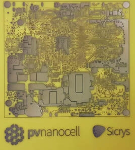
PV Nano Cell Ltd, an innovative provider of inkjet-based conductive digital printing solutions and producer of conductive digital inks, announced that it has launched a new, general-purpose conductive gold ink to be used with inkjet and aerosol printing.
The new gold ink was specially developed to meet requirements made by customers and covers a wide range of applications. The company expects many uses for the ink including with PCB, connectors, switch and relay contacts, soldered joints, plating and wire bonding. The current subtractive and plating technologies of gold are highly expensive and complicated to use. The new ink now enables a simple, digital, additive, mass-production technology.
This additive technology guarantees the best manufacturing cost while offering a new level of design flexibility and product time-to-market. This new commercial ink will complement the company’s existing product line of silver, copper and dielectric inks.
PV Nano Cell’s Chief Executive Officer, Dr. Fernando de la Vega, commented, “For digital printed electronics in mass production to become the mainstream, additional inks and printing solutions need to be developed to address inherent challenges. Such challenges include for example reducing corrosion, enabling soldering and wire bonding, etc. The ability to inkjet or aerosol-print our gold ink is a significant step forward to further enable digital printing to become widely used. This new product will drive new, high-performance and reliable electronics in the most competitive offering. As gold is used in virtually all advanced electronic devices, the market potential is overwhelming, particularly given the cost-performance bundle our new gold ink offers. We further plan to optimize the ink to our DemonJet Printer that is capable of printing up to 10 inks at the same time. Our end goal is for the printer to support our silver, dialectic, gold and resistor inks to allow customers to print a variety of pioneer products. Our advanced development of printed embedded passive components is now complemented by this new gold ink.“
As recently published earlier this month, the company announced that it has signed, under NDA, an agreement with a well-known, world-leading multinational healthcare company to develop a new inkjet printing technology for the fabrication of sensors using resistor and gold inks. This new general-purpose gold ink, differs in performance and optimization from the ink developed for healthcare applications.
PV Nano Cell’s Chief of Business Development Officer, Mr. Hanan Markovich commented, “We are being contacted frequently by customers actively looking for high-performance gold ink. Having discussed customers’ needs, we learned the market requires gold ink to address significant manufacturing issues. We further realized, current technologies and alternatives are highly expensive, inefficient and hard to implement, suggesting a great business potential. The new gold ink developed by PV Nano Cell solves real problems for customers, in an affordable way. We are now finalizing the preliminary orders and working on expanding the pipeline.“
Share on:


Testimonial
"The I-Connect007 team is outstanding—kind, responsive, and a true marketing partner. Their design team created fresh, eye-catching ads, and their editorial support polished our content to let our brand shine. Thank you all! "
Sweeney Ng - CEE PCBSuggested Items
Trouble in Your Tank: Minimizing Small-via Defects for High-reliability PCBs
08/27/2025 | Michael Carano -- Column: Trouble in Your TankTo quote the comedian Stephen Wright, “If at first you don’t succeed, then skydiving is not for you.” That can be the battle cry when you find that only small-diameter vias are exhibiting voids. Why are small holes more prone to voids than larger vias when processed through electroless copper? There are several reasons.
The Government Circuit: Navigating New Trade Headwinds and New Partnerships
08/25/2025 | Chris Mitchell -- Column: The Government CircuitAs global trade winds continue to howl, the electronics manufacturing industry finds itself at a critical juncture. After months of warnings, the U.S. Government has implemented a broad array of tariff increases, with fresh duties hitting copper-based products, semiconductors, and imports from many nations. On the positive side, tentative trade agreements with Europe, China, Japan, and other nations are providing at least some clarity and counterbalance.
How Good Design Enables Sustainable PCBs
08/21/2025 | Gerry Partida, Summit InterconnectSustainability has become a key focus for PCB companies seeking to reduce waste, conserve energy, and optimize resources. While many discussions on sustainability center around materials or energy-efficient processes, PCB design is an often overlooked factor that lies at the heart of manufacturing. Good design practices, especially those based on established IPC standards, play a central role in enabling sustainable PCB production. By ensuring designs are manufacturable and reliable, engineers can significantly reduce the environmental impact of their products.
50% Copper Tariffs, 100% Chip Uncertainty, and a Truce
08/19/2025 | Andy Shaughnessy, I-Connect007If you’re like me, tariffs were not on your radar screen until a few months ago, but now political rhetoric has turned to presidential action. Tariffs are front-page news with major developments coming directly from the Oval Office. These are not typical times. President Donald Trump campaigned on tariff reform, and he’s now busy revamping America’s tariff policy.
Global PCB Connections: Understanding the General Fabrication Process—A Designer’s Hidden Advantage
08/14/2025 | Markus Voeltz -- Column: Global PCB ConnectionsDesigners don’t need to become fabricators, but understanding the basics of PCB fabrication can save you time, money, and frustration. The more you understand what’s happening on the shop floor, the better you’ll be able to prevent downstream issues. As you move into more advanced designs like HDI, flex circuits, stacked vias, and embedded components, this foundational knowledge becomes even more critical. Remember: the fabricator is your partner.