


 It’s Only Common Sense: Your Biggest Competitor Is Complacency
 The Chemical Connection: Onshoring PCB Production—Daunting but Certainly Possible
 Marcy’s Musings: The Legislative Outlook—Helping or Hurting?


Nano Dimension Sells Two DragonFly IV 3D-AME Systems to Defense and Government Agencies
December 6, 2021 | Nano Dimension Ltd.Estimated reading time: 2 minutes
Nano Dimension Ltd., an industry-leader in Additively Manufactured Electronics (AME), Printed Electronics (PE), and Micro Additive Manufacturing (Micro-AM), announced that it has sold the first two DragonFly IV 3D-AME Printers, in addition to the two machines that have completed beta sites processes with other leading customers.
Nano Dimension is the leading provider of intelligent machines for the fabrication of AME. The new DragonFly IV system, combined with FLIGHT software, delivers new levels of quality, efficiency, and print resolution in the 3D printed electronics sector, providing increased flexibility to design any 3D geometry and create innovative new products.
DragonFly IV is a Dielectric and Conductive-Materials Additive Manufacturing System aimed for fabrication of High-Performance Electronic Devices (Hi-PEDs®) by depositing the proprietary materials simultaneously, while concurrently integrating in-situ capacitors, antennas, coils, transformers, and electro-mechanical components.
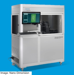
DragonFly IV 3D-AME Printer
DragonFly IV delivers improved accuracy of traces, spacing, and vias, improved PCB product quality, and the ability to design and produce 3D Hi-PEDs® in a one-step production process.
New capabilities include:
- Integration with Nano Dimension’s new FLIGHT software
- Integration of 3D elements in PCB
- 3D designed Hi-PEDs®
- Support of HDI level elements
- 75µm traces; 100µm spacing; 150µm via
- Enhanced print quality, optimizing yield with predictable conductivity
- Low thickness variation
FLIGHT Software Package
Nano Dimension’s new FLIGHT software suite provides a comprehensive first-of-a-kind ability to incorporate ECAD designs into real 3D MCAD designs, as well as intelligent verification, slicing, and job control solutions. FLIGHT enables the 3D design of electrical and mechanical features in 3-dimensions while ensuring that the new product designs comply with the system’s requirements and can then proceed directly to fabrication on the DragonFly IV.
The Flight Software Suite consists of 3 components:
1-FLIGHT Plan: Allows designers to develop viable 3D AME using both existing 2D design data, and novel 3D data. Tests show that this reduces the 3D AME design time by up to 10 times.
- Integrates 3D MCAD and ECAD capabilities for 3D Electro-Mechanical design
- Imports existing designs from major ECAD systems
- Enables the use of customers’ existing design tools
2-FLIGHT Check: This application enables design rule checks so that the designs meet the DragonFly IV requirements and are ready for printing.
- Unifies design rules for ECAD that meet the constraints of DragonFly IV
- Reduces design iteration cycles
3-FLIGHT Control: Delivers an entirely new pre-production solution that enables concurrent fabrication of both 2D and 3D multi-material Hi- PEDs®, improving productivity.
- Integrates system and job management toolsets
- Supports new file formats (STL & ODB++)
- Improves user experience through better rendering accuracy and user interface
Share on:


Testimonial
"Advertising in PCB007 Magazine has been a great way to showcase our bare board testers to the right audience. The I-Connect007 team makes the process smooth and professional. We’re proud to be featured in such a trusted publication."
Klaus Koziol - atgSuggested Items
American Standard Circuits Launches 50th 77-Second Webinar
10/27/2025 | American Standard CircuitsAnaya Vardya, President and CEO of American Standard Circuits/ASC Sunstone Circuits is pleased to announce that they have recently unveiled their 50th 77-second webinar.
Peters, Starteam, and Würth Elektronik Team Up For Digital Coating Technology
10/23/2025 | PetersUnder this heading, the PCB manufacturers Starteam and Würth Elektronik, along with Peters as inkjet coating supplier, have taken the initiative and worked together for months in trusting and target-oriented cooperation, to promote this innovative digital coating technology for solder resists and establish it on the market.
AI Triggers Next Paradigm Shift in PDN
10/23/2025 | Istvan Novak, SamtecArtificial intelligence (AI), together with machine learning (ML), is creating an unprecedented surge of computing and networking infrastructure needs. This, in turn, has dramatically increased the power consumption of computing and networking chips.
SEMICON Japan 2025 to Spotlight Sustainability in AI and Semiconductor Innovation
10/22/2025 | SEMISEMICON Japan 2025, the largest gathering of leaders from the microelectronics manufacturing supply chain in Japan, will bring together more than 1,200 exhibitors showcasing semiconductor solutions from December 17-19 at Tokyo Big Sight.
Zuken Announces ZIW Americas 2026 in Dallas
10/21/2025 | ZukenZuken USA, Inc., a global leader in electrical and electronic design automation, announced Zuken Innovation World (ZIW) Americas 2026, the company’s premier global conference dedicated to advancing the future of electrical and electronic product design. ZIW 2026 will be held June 9-11 in Dallas, Texas.