


 Global PCB Connections: Rigid-flex and Flexible PCBs—The Backbone of Modern Electronics
 Flexible Thinking: The Key to a Successful Flex Circuit Design Transfer
 Happy’s Tech Talk #29: Bend-to-Install Semi-flex FR-4


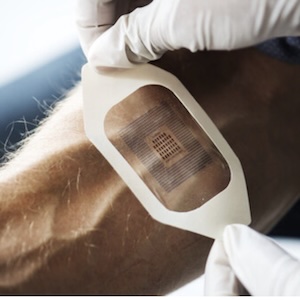
Testing Flexible Circuit Assemblies
January 18, 2022 | Andy Shaughnessy, Design007 MagazineEstimated reading time: 3 minutes

I recently spoke with Bert Horner of the Test Connection Inc., about the current state of flex and rigid-flex assembly testing. He explained some of the differences between testing flex and rigid PCBs, the requirements for testing specialties such as high-voltage flex, and the added demands of handling flexible circuits.
Andy Shaughnessy: Bert, tell us about your company and the kinds of test equipment you’ve developed for flexible and rigid-flex circuits. I understand you also provide test services too; do you offer testing for flex?
Bert Horner: The Test Connection Inc., is a full services test engineering and test service that offers different test solutions to test rigid and rigid flex circuits. For prototype or lower volume assemblies, we have flying probe and boundary scan solutions and for the production testing, we have in-circuit test and functional test solutions from partners like Teradyne, Keysight, and National Instruments. TTCI works with fixture partners to offer custom in-house solutions to support and access these challenging assemblies.
Shaughnessy: What are the most common tests for flexible circuit assemblies as well as the biggest challenges? Do high-voltage flexible circuits require a different set of tests than the rest?
Horner: For flying probe testing (FPT), in-circuit testing (ICT) and functional test (FT), the biggest challenge is the tooling for testing the assembly. For the FPT, the handling of the unit under test (UUT) is one of the biggest challenges. This can still be a challenge if the assembly is thin and flimsy, so tooling could still be required. If ICT and FT are done on a fixture or bed-of-nails (BoN), we don’t want to introduce stress to the UUT, so “zero flex” fixturing with finite element analysis (FEA) and strain gauge might be needed, which also adds time and cost. In FT, we see that in high-voltage testing, the biggest challenge is making sure the equipment that will be testing assembly can handle the proper testing requirements. This is about the same set-up as a rigid board, but we haven’t seen too many applications that have this as a requirement.
Shaughnessy: What are some of the biggest differences between testing a flexible circuit and a traditional rigid PCB?
Horner: The physical handling is the biggest challenge in testing flex or rigid-flex circuitry. We often have to develop a custom carrier or handling fixture to test flex or rigid-flex assemblies to help with stability and support.
Shaughnessy: We’ve seen flex and rigid-flex explode in the last decade, and now flex can be found in many household and handheld devices. What trends are you seeing in the world of flex?
Horner: Test access is more of a challenge with accessing the test assemblies through connectors and SMT device “toes” of the solder joints with the assemblies going into two completely different directions. The wearable, handheld, and space applications are getting smaller, but the defense backplanes are in some cases getting larger.
Shaughnessy: How much of your job involves educating new customers about flex and testing?
Horner: We are not doing much with educating the customer on how they want to test flex circuitry, but rather showing them strengths and weaknesses in the test solutions they are choosing or that they have available to test their assemblies. If we are looking at multiple test and inspection tools to get the most coverage on these assemblies, the education becomes about what is best for manufacturing. We both learn preferences of tools that are available.
Shaughnessy: Is there anything else you’d like to add?
Horner: There are more similarities of testing flex circuitry and conventional rigid circuitry, the access, and the handling are where we see the challenge.
Shaughnessy: Thanks for your time, Bert.
Horner: Thank you for the opportunity, Andy.
This interview originally appeared in the January 2022 issue of Design007 Magazine.
Share on:


Testimonial
"We’re proud to call I-Connect007 a trusted partner. Their innovative approach and industry insight made our podcast collaboration a success by connecting us with the right audience and delivering real results."
Julia McCaffrey - NCAB GroupSuggested Items
Rehm Wins Mexico Technology Award for CondensoXLine with Formic Acid
10/17/2025 | Rehm Thermal SystemsModern electronics manufacturing requires technologies with high reliability. By using formic acid in convection, condensation, and contact soldering, Rehm Thermal Systems’ equipment ensures reliable, void-free solder joints — even when using flux-free solder pastes.
Indium Experts to Deliver Technical Presentations at SMTA International
10/14/2025 | Indium CorporationAs one of the leading materials providers to the power electronics assembly industry, Indium Corporation experts will share their technical insight on a wide range of innovative solder solutions at SMTA International (SMTAI), to be held October 19-23 in Rosemont, Illinois.
Knocking Down the Bone Pile: Revamp Your Components with BGA Reballing
10/14/2025 | Nash Bell -- Column: Knocking Down the Bone PileBall grid array (BGA) components evolved from pin grid array (PGA) devices, carrying over many of the same electrical benefits while introducing a more compact and efficient interconnect format. Instead of discrete leads, BGAs rely on solder balls on the underside of the package to connect to the PCB. In some advanced designs, solder balls are on both the PCB and the BGA package. In stacked configurations, such as package-on-package (PoP), these solder balls also interconnect multiple packages, enabling higher functionality in a smaller footprint.
Indium to Showcase High-Reliability Solder and Flux-Cored Wire Solutions at SMTA International
10/09/2025 | Indium CorporationAs one of the leading materials providers in the electronics industry, Indium Corporation® will feature its innovative, high-reliability solder and flux-cored wire products at SMTA International (SMTAI), to be held October 19-23 in Rosemont, Illinois.
‘Create your Connections’ – Rehm at productronica 2025 in Munich
10/08/2025 | Rehm Thermal SystemsThe electronics industry is undergoing dynamic transformation: smart production lines, sustainability, artificial intelligence, and sensor technologies dominate current discussions.