


 Trouble in Your Tank: Causes of Plating Voids, Pre-electroless Copper
 Dan’s Biz Bookshelf: ‘Growth Hacker Marketing’
 Happy’s Tech Talk #38: Novel Metallization for UHDI


Can Electronics Manufacturing Join the Digital Age, Asks IDTechEx
March 29, 2023 | PRNewswireEstimated reading time: 3 minutes
Asked whether electronics is a 'digital technology', almost everyone would reply in the affirmative. However, while printed circuit boards (PCBs) enable digital technologies, the manufacturing processes used to produce them are still largely analog.
'Digital manufacturing' refers to any method that is directly controlled by a computer – simply using software in the design process doesn't count. Well-known examples are CNC (computer numerical control) machining, a subtractive method in which a rotational cutting tool selectively removes material, and 3D printing, an additive method that involves selective deposition of metal, plastic, or even ceramic. In both cases, direct computer control means that every part produced can have a different design and even that the design can be adjusted once manufacturing is in progress.
In contrast, conventional PCB manufacturing takes an analog approach. The desired pattern is transferred to a mask that is used for photolithography. Regions of material, typically copper laminate on a PCB, that are not coated with the patterned resist are then removed with an etchant. While this approach enables efficient high-yield production, introducing digital manufacturing methods would bring additional benefits.
Why Do We Need Digital Electronics Manufacturing?
Arguably, the main benefit of digital over analog manufacturing is that every item can be different with no additional setup time or costs. This is why inkjet printers (digital) are used at home since only a single copy is typically needed, whereas offset printing (analog) is used for mass-produced newspapers. With electronics, digital manufacturing enables rapid prototyping, accelerating the design process. It facilitates mass customization, where every circuit has a different design if desired without dramatically increasing production costs. Furthermore, high-resolution digital manufacturing methods can be used in conjunction with conventional photolithography to repair any unwanted circuit breaks.
Digital Manufacturing Methods for Electronics
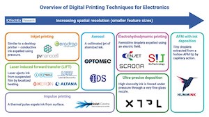
Interest in digital manufacturing methods for electronics has increased rapidly over recent years. While inkjet printing is by far the best-established method of digitally depositing conductive ink, there are a variety of emerging techniques that are both digital and additive. They all offer the direct control of digital manufacturing while spanning a range of throughputs, resolutions, material viscosity, and substrate dimensionality.
Print-then-plate utilizes inkjet printing of a thin layer of silver nanoparticle conductive ink to selectively pattern the substrate. This 'seed layer' is then fully metalized by electroless plating, producing a copper circuit. This method is already used for mass production. It combines the customizability of digital manufacturing, the reduced waste of additive manufacturing, and the conductivity of copper metal (rather than printed conductive ink).
Laser induced forward transfer (LIFT) can be regarded as a hybrid of laser direct structuring (LDS) and inkjet printing. Briefly, a laser heats conductive ink coated underneath a 'transfer plate', with evaporating solvent ejecting the ink. The lack of nozzle is a major benefit since it enables viscous inks typically used for screen printing to be used. There is potential for LIFT to be used in tandem with R2R production, enabling rapid, cost-effective production of customized circuits.
Aerosol printing is a relatively established technique that is well suited to printing onto 3D surfaces. A low-viscosity ink is atomized and formed into a thin collimated jet within a gas sheath layer, enabling resolutions as fine as 10 um with a working distance of up to 5cm. It's already being used in the semiconductor packaging production process and will soon be applied to larger area conformal surfaces such as automotive glass.
Electrohydrodynamic printing (EHD) uses an electric field to 'pull' ink from a nozzle rather than relying on pressure to 'push' out the ink. Capable of traces as narrow as 1um, this technique is currently being used to repair defects in TFT backplanes. An emerging approach is to combine hundreds of individually addressable nozzles within a single MEMS (micro electromechanical system) chip promises to break the resolution/throughput trade-off for small-scale additive electronics manufacturing.
Impulse printing is an innovative technique in the early stages of development that promises high throughput printing onto 3D surfaces, such as the edges of glass backplanes or 2.5D semiconductor packaging. The approach utilizes a rapid heat pulse from a controllable array of heating elements to expel ink from a flat 'transfer surface' onto the target object. Since no nozzle is used, ink can simultaneously be expelled from across the heated 'transfer surface'.
Share on:


Suggested Items
Creative Electron Strengthens Leadership Team with Strategic Appointments in Marketing and SMT Business Unit
05/08/2025 | Creative ElectronCreative Electron, the largest U.S. manufacturer of X-ray inspection systems for the electronics industry, is proud to announce the addition of two seasoned leaders to its executive team: Wagner Lima as Marketing Director and Giancarlo De La Garza as SMT Business Unit Director.
LG Electronics India Limited Begins Construction of Its Third Manufacturing Plant in India
05/08/2025 | BUSINESS WIRELG Electronics India Ltd. (LGEIL) announced the commencement of construction of its new manufacturing facility in Sri City, Andhra Pradesh today at a ceremony graced by the presence of Shri Nara Lokesh, Hon'ble Minister for Information Technology, Electronics and Communications.
Scanfil Boosts Investment in Electronics Manufacturing in the US
05/08/2025 | BUSINESS WIREScanfil is investing in a second electronics manufacturing line in Atlanta, Georgia, USA. The demand for manufacturing electronics in the USA has increased over the past two years and is expected to continue growing.
IPC Strengthens Global Focus with Promotion of Sanjay Huprikar to Chief Global Officer
05/08/2025 | IPCIPC, the global electronics association, announces the promotion of Sanjay Huprikar to chief global officer. This newly created position reflects the association’s forward-looking strategy and industry needs to strengthen the electronics supply chain.
IPC White Paper Maps the Regulatory Terrain for Electronics Suppliers in E-Mobility Sector
05/07/2025 | IPCElectronics suppliers supporting the rapidly growing e-mobility sector are facing a dramatic escalation in environmental and social governance (ESG) compliance expectations. A new white paper from IPC’s e-Mobility Quality and Reliability Advisory Group provides a comprehensive overview of the evolving regulatory landscape and outlines the data infrastructure needed to stay ahead.