


 It’s Only Common Sense: Marketing Isn’t Fluff, It’s Ammunition
 Driving Innovation: Mechanical and Optical Processes During Rigid-flex Production
 The Chemical Connection: Onshoring PCB Production—Daunting but Certainly Possible


New SIA Map Highlights Broad U.S. Semiconductor Ecosystem
March 29, 2023 | SIAEstimated reading time: 1 minute
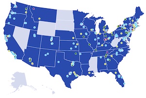
The semiconductor ecosystem in the United States is broad and diverse, as illustrated by SIA’s new U.S. Semiconductor Ecosystem Map, a first-of-its-kind tool that allows users to explore industry activities across the country, including nearly 500 locations in 42 states. This expansive ecosystem is comprised of semiconductor manufacturing, chip design, intellectual property and chip design software providers, semiconductor materials and manufacturing equipment, and research and development, including university R&D partners of the Semiconductor Research Corporation (SRC) and the National Nanotechnology Coordinated Infrastructure (NNCI).
Of particular note, the U.S. Semiconductor Ecosystem Map highlights announced company investments for new and expansion semiconductor ecosystem projects. These projects cover a range of activities needed to bolster the U.S. chip ecosystem, including new, expanded, or upgraded fabs in various semiconductor segments (e.g., advanced logic, memory, analog, and legacy chips), semiconductor equipment facilities, and facilities to produce key materials used in the chip manufacturing process. From the time the CHIPS Act was introduced in the Spring of 2020 through the months following its enactment in August 2022, companies in the semiconductor ecosystem announced dozens of projects to increase manufacturing capacity in the U.S. As of March 2023, some highlights of announcements spurred by the CHIPS Act include:
- Over $210 billion in new private investments announced across 19 states to increase domestic manufacturing capacity
- Over 50 new semiconductor ecosystem projects announced across the U.S., including the construction of new fabs, expansions of existing sites, and facilities that supply the materials and equipment used in chip manufacturing
- 44,000 new high-quality jobs announced in the semiconductor ecosystem as part of the new projects, which will support many more jobs throughout the broader U.S. economy
As the CHIPS Act incentives and R&D programs continue to be implemented, SIA’s U.S. Semiconductor Ecosystem Map will be updated to reflect the ever-growing domestic semiconductor footprint.
Share on:


Testimonial
"Your magazines are a great platform for people to exchange knowledge. Thank you for the work that you do."
Simon Khesin - Schmoll MaschinenSuggested Items
Electronics Manufacturing Powers U.S. Growth, Supporting 5.2 Million Jobs and $1.8 Trillion in Output
11/03/2025 | Global Electronics AssociationNew report from Global Electronics Association shows electronics industry contributes $853 billion to GDP and delivers average annual wages exceeding $156,000, reinforcing its role as a pillar of U.S. economic resilience.
TTM Technologies Receives Two Awards from the Global Electronics Association at the 2025 IPC CEMAC Conference
11/03/2025 | Globe NewswireTTM Technologies, Inc. announced that two of its team members received prestigious Asia Steering Committee Outstanding Service Awards from the Global Electronics Association (formerly named IPC connecting global electronics industry) at the 2025 IPC CEMAC Electronics Manufacturing Annual Conference in Shanghai.
SMT007 Magazine November 2025: Inside Mexico’s Rise as an Electronics Manufacturing Leader
11/03/2025 | I-Connect007 Editorial TeamMexico isn’t just part of the electronics manufacturing conversation—it’s leading it. From growing investments to cross-border collaborations, Mexico is fast becoming the center of electronics in North America. In this issue, we uncover why Mexico is earning global recognition. From top-ranked manufacturing capabilities to expanding partnerships that reach far beyond the U.S.
Henger Microelectronics Expands Global Footprint with Major Equipment Shipment to Southeast Asia
10/31/2025 |Henger Microelectronics has reached a major milestone in its global expansion strategy with the successful shipment of advanced plasma etching and cleaning systems, along with automation equipment, to multiple countries and regions across Southeast Asia. This achievement marks a significant step forward in the company’s international growth and reinforces its position as a leading force in the global plasma equipment industry.
PCBAA Names Industry Veteran Dan Weber to Board of Directors
10/31/2025 | PCBAAThe Printed Circuit Board Association of America has added Dan Weber, Executive Vice President and General Counsel at TTM Technologies, to the PCBAA board of directors.