


 The Marketing Minute: Marketing With Layers
 The Right Approach: Electro-Tek—A Williams Family Legacy, Part 1
 It’s Only Common Sense: If You’re Not Differentiated, You’re Dead


The Birth of the Printed Circuit Board
May 23, 2023 | Barry Matties and Nolan Johnson, I-Connect007Estimated reading time: 2 minutes
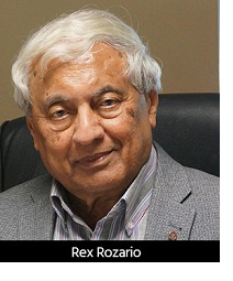
Every industry has a beginning, and we are lucky to have Rex Rozario here to share the story of how the printed circuit board industry got its start. I-Connect007 chatted with Rex recently about how he became involved with circuit board inventor Dr. Paul Eisler.
Barry Matties: Let’s start at the beginning, Rex. My understanding is you were there when circuit boards were first being manufactured.
Rex Rozario: You're correct. Fortunately for me, when I left university, my first job was with a company called The Telegraph Condenser Company; they had just acquired the first license from Paul Eisler. He developed the printed circuit in a shed in London, circa 1940; they were single-sided boards. He had the patents in 1948 and issued five licenses. We (The Telegraph Condenser Company) were the first to get a license.
Eisler later joined Technograph and worked there for some time. Eventually, Technograph and Telegraph merged.
Matties: Would you say you were the first company to produce a licensed printed circuit board?
Rozario: Technically, we were the first company in the UK to manufacture PCBs. Eisler sold one license to the UK and four others to the U.S. We could appoint other people as well, if they wanted to manufacture under our license.
Matties: So, how did you get involved?
Rozario: Whilst studying for my degree at university, I was lucky to obtain a work/study job in my spare time in a development lab with Daly Condensers Ltd. (UK) where I learned all about manufacturing electrical condensers. This gave me the opportunity, after obtaining my university degree, to apply to the UK's largest condenser manufacturer, The Telegraph Condenser Co., which employed me as a development technician. Three weeks into my new job, I took a pre-arranged vacation for two weeks. When I returned, I was met by a senior director and was marched into the office of the managing director who was already addressing five men. The managing director informed us that Telegraph had just obtained the first license in the world from the inventor Dr. Paul Eisler, who was also engaged by Telegraph as a consultant. I was invited to join the five specialists which Telegraph had tapped to form this new team with Dr. Eisler. We were given 5,000 square feet of a surplus building to further develop and introduce printed circuits to replace manual wiring. This period was circa 1953.
In the beginning, we had to shop around for everything, from the base laminate to the copper foil. We did all that within our team, and then suddenly the printed circuit developed in the UK went from a single- to a double-sided board. For the double sided, we used eyelets until through-hole [electroless copper plating] came along.
Matties: You were along for the journey the whole way.
Rozario: I was just lucky to be there.
To read this entire conversation, which appeared in the May 2023 issue of PCB007 Magazine, click here.
Share on:


Testimonial
"Advertising in PCB007 Magazine has been a great way to showcase our bare board testers to the right audience. The I-Connect007 team makes the process smooth and professional. We’re proud to be featured in such a trusted publication."
Klaus Koziol - atgSuggested Items
Episode 6 of Ultra HDI Podcast Series Explores Copper-filled Microvias in Advanced PCB Design and Fabrication
10/15/2025 | I-Connect007I-Connect007 has released Episode 6 of its acclaimed On the Line with... American Standard Circuits: Ultra High Density Interconnect (UHDI) podcast series. In this episode, “Copper Filling of Vias,” host Nolan Johnson once again welcomes John Johnson, Director of Quality and Advanced Technology at American Standard Circuits, for a deep dive into the pros and cons of copper plating microvias—from both the fabricator’s and designer’s perspectives.
Nolan’s Notes: Tariffs, Technologies, and Optimization
10/01/2025 | Nolan Johnson -- Column: Nolan's NotesLast month, SMT007 Magazine spotlighted India, and boy, did we pick a good time to do so. Tariff and trade news involving India was breaking like a storm surge. The U.S. tariffs shifted India from one of the most favorable trade agreements to the least favorable. Electronics continue to be exempt for the time being, but lest you think that we’re free and clear because we manufacture electronics, steel and aluminum are specifically called out at the 50% tariff levels.
MacDermid Alpha & Graphic PLC Lead UK’s First Horizontal Electroless Copper Installation
09/30/2025 | MacDermid Alpha & Graphic PLCMacDermid Alpha Electronics Solutions, a leading supplier of integrated materials and chemistries to the electronics industry, is proud to support Graphic PLC, a Somacis company, with the installation of the first horizontal electroless copper metallization process in the UK.
Electrodeposited Copper Foils Market to Grow by $11.7 Billion Over 2025-2032
09/18/2025 | Globe NewswireThe global electrodeposited copper foils market is poised for dynamic growth, driven by the rising adoption in advanced electronics and renewable energy storage solutions.
MacDermid Alpha Showcases Advanced Interconnect Solutions at PCIM Asia 2025
09/18/2025 | MacDermid Alpha Electronics SolutionsMacDermid Alpha Electronic Solutions, a global leader in materials for power electronics and semiconductor assembly, will showcase its latest interconnect innovations in electronic interconnect materials at PCIM Asia 2025, held from September 24 to 26 at the Shanghai New International Expo Centre, Booth N5-E30