


 The Marketing Minute: Marketing With Layers
 The Right Approach: Electro-Tek—A Williams Family Legacy, Part 1
 It’s Only Common Sense: If You’re Not Differentiated, You’re Dead


Analog Devices Further Strengthens its South-East Asia Operations with New Singapore Facility
May 31, 2023 | ACN NewswireEstimated reading time: 2 minutes
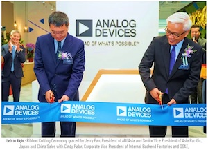
Analog Devices, Inc., a global semiconductor leader, announced the launch of a new state-of-the-art, environmentally friendly, 38,951 sq. ft. facility in Singapore. Located within the Kallang Industrial Park, the facility is planned to serve as a central hub for the more than 200 employees working in Singapore in key divisions of the company, including research and development, test engineering, sales, and manufacturing. ADI established its first location in Singapore in 1995 and has steadily grown its operations and workforce since then. This new strategic investment aligns with the company's global expansion plans, which include enhancing its capabilities in the Asia Pacific region.
"Our new facility is an important milestone in ADI's global growth strategy," said Jerry Fan, President of Asia for ADI. "Enhancing our capabilities in Singapore is vital to leveraging the country's superb talent pool and advanced manufacturing capabilities to serve our regional and global customers' needs. Our investment reinforces ADI's presence within Singapore's thriving semiconductor ecosystem, which is supported by the nation's digital growth initiatives."
The new facility features a more spacious and advanced laboratory to foster interaction between the research and development team as well as customers in the region. Through this forum for the exchange of ideas, ADI and its customers plan to deepen their collaboration and deliver innovative products for the Intelligent Edge. In addition, a dedicated space has been allocated for test development purposes within the new facility, custom-tailored to accommodate multiple automated test equipment (ATE) stations. These on-site testing stations are designed to enable faster initial testing of ADI's state-of-the-art products and accelerate the timeline of ADI engineering's ability to meet customers' toughest challenges.
Fan continued, "Customer intimacy, business strategy, engineering processes, manufacturing capabilities, and problem-solving are essential for creating long-term value for our customers. We are confident the environment within our new facility will help us deliver the kind of innovation that leads to breakthrough products and services, and we believe it will have a lasting impact on the region's ongoing digital transformation journey."
Location selection and build criteria for the site prioritized accessibility and sustainability. The new office is bicycle-friendly, close to public transportation, and is directly accessible via expressways. Recyclable materials were used throughout construction, and energy efficient AC, lighting, and water systems are all part of its advanced building automation system. Low carbon footprint materials were an integral part of the biophilic interior design. The office building is Green Mark Platinum-certified and expected to get LEED Gold certification by July 2023.
Share on:


Testimonial
"Advertising in PCB007 Magazine has been a great way to showcase our bare board testers to the right audience. The I-Connect007 team makes the process smooth and professional. We’re proud to be featured in such a trusted publication."
Klaus Koziol - atgSuggested Items
NextFlex Announces New Affiliated Alabama ‘Node’ to Support Growing National Hybrid Electronics Community
10/16/2025 | PRNewswireNextFlex®, America's Hybrid Electronics Manufacturing Innovation Institute, announced the launch of a new Alabama Node. The Alabama Node will accelerate the commercialization of hybrid electronics by boosting innovation, technology transition, and adoption.
Myrias Optics, Pixelligent Announce Strategic Manufacturing Partnership
10/16/2025 | PRNewswireMyrias Optics, a pioneering manufacturer of flat optics , and Pixelligent Technologies LLC, the leading manufacturer of high refractive index (RI) nanocomposites for next-gen electronics, announced that they have entered into a strategic manufacturing partnership.
NOTE Posts Interim Report Q3 2025
10/16/2025 | NOTE ABNOTE AB reported renewed growth and continued strong profitability in Q3 2025, with sales rising to SEK 830 million and an adjusted operating margin of 9.3%.
HANZA Wins Drone Order Under the LYNX Program
10/15/2025 | HANZAHANZA has received an initial order worth approximately SEK 40 million from a high-tech company that develops and sells drones for both civilian and defense-related applications.
SAMI Advanced Electronics Company Launches “Remal” Computer Manufacturing Project in Partnership with HP and Foxconn
10/15/2025 | SAMI-AECSAMI Advanced Electronics Company (SAMI-AEC), a wholly owned subsidiary of Saudi Arabian Military Industries (SAMI), proudly announced the launch of the “Remal” project for computer manufacturing, in strategic partnership with HP and Foxconn.