


 Global PCB Connections: Rigid-flex and Flexible PCBs—The Backbone of Modern Electronics
 Flexible Thinking: The Key to a Successful Flex Circuit Design Transfer
 Happy’s Tech Talk #29: Bend-to-Install Semi-flex FR-4


Challenges of DFM Analysis for Flex and Rigid-Flex Design, Part 3
June 14, 2023 | Mark Gallant, DownStream TechnologiesEstimated reading time: 2 minutes

(Editor’s note: This is the final installment of a three-part series. To read Part 2, click here.)
What a True Rigid-flex DFM Analysis Solution Must Include
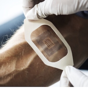
DFM analysis tools for the last several decades have focused on a typical rigid PCB or some variant. While many standard DFM constraints are applicable, flex has many unique requirements that cannot be addressed with typical DFM analysis. Flex and rigid-flex DFM must be targeted toward the unique materials and processes used to produce flex and rigid-flex designs.
One such example is board outline vs. layer profile. Some CAD systems do not support boundaries on a per layer basis. For most rigid-flex designs, all that is provided is a cumulative board outline that is the extent of all layer shapes. Without a defined boundary per layer, there may be no prevention of routing traces or placing components outside, or off of, a layer in the CAD system. The CAD DRC may also miss these items because they are within the boundary of the cumulative board outline. Having a DFM tool capable of analyzing each layer against its unique profile can detect when conductors are outside, or off of, their respective layers.
Here is a categorized list of the types of analyses and features a flex or rigid-flex DFM tool should have.
1. Trace fracture
Trace or copper fracture in bend areas. Some examples include presence of trace corners, width transitions, or traces non-perpendicular to the bend axis in a bend area. Also, I-beaming where traces are coincident on adjacent flexible layers.
2. Delamination
Pads or vias in bend areas with improper pad shapes or coverlay exposures. When it is required to have vias or other pads in bend areas, special care must be taken when designing the coverlay to reduce delamination potential. Often in these conditions, the coverlay overlaps the pad area to prevent delamination. In other designs, pads are adorned with tabs to extend under the coverlay.
3. Tearing
The absence of tear stops on slits or inside corners. Copper segments, arcs, circles, or other shapes are added to prevent tear around slits or inside corners.
4. Squeeze out
Epoxy leakage onto adjacent copper or other layer surfaces. In order to prevent epoxy squeeze out, a perimeter air gap or fence must be present around adjacent layer content. For example, a larger annular ring may be required on the epoxy layer than its corresponding coverlay annular ring. This prevents epoxy from squeezing out onto adjacent copper or traces.
5. Button plating
Absence of exposures in coverlay for vias. The most common method of plating vias in a bend area is button plating. This requires vias to be plated have an exposure on their adjacent coverlay. Absence of an exposure on the coverlay would prevent plating.
To read this entire article, which appeared in the June 2023 issue of Design007 Magazine, click here.
Share on:


Testimonial
"In a year when every marketing dollar mattered, I chose to keep I-Connect007 in our 2025 plan. Their commitment to high-quality, insightful content aligns with Koh Young’s values and helps readers navigate a changing industry. "
Brent Fischthal - Koh YoungSuggested Items
Episode 6 of Ultra HDI Podcast Series Explores Copper-filled Microvias in Advanced PCB Design and Fabrication
10/15/2025 | I-Connect007I-Connect007 has released Episode 6 of its acclaimed On the Line with... American Standard Circuits: Ultra High Density Interconnect (UHDI) podcast series. In this episode, “Copper Filling of Vias,” host Nolan Johnson once again welcomes John Johnson, Director of Quality and Advanced Technology at American Standard Circuits, for a deep dive into the pros and cons of copper plating microvias—from both the fabricator’s and designer’s perspectives.
Nolan’s Notes: Tariffs, Technologies, and Optimization
10/01/2025 | Nolan Johnson -- Column: Nolan's NotesLast month, SMT007 Magazine spotlighted India, and boy, did we pick a good time to do so. Tariff and trade news involving India was breaking like a storm surge. The U.S. tariffs shifted India from one of the most favorable trade agreements to the least favorable. Electronics continue to be exempt for the time being, but lest you think that we’re free and clear because we manufacture electronics, steel and aluminum are specifically called out at the 50% tariff levels.
MacDermid Alpha & Graphic PLC Lead UK’s First Horizontal Electroless Copper Installation
09/30/2025 | MacDermid Alpha & Graphic PLCMacDermid Alpha Electronics Solutions, a leading supplier of integrated materials and chemistries to the electronics industry, is proud to support Graphic PLC, a Somacis company, with the installation of the first horizontal electroless copper metallization process in the UK.
Electrodeposited Copper Foils Market to Grow by $11.7 Billion Over 2025-2032
09/18/2025 | Globe NewswireThe global electrodeposited copper foils market is poised for dynamic growth, driven by the rising adoption in advanced electronics and renewable energy storage solutions.
MacDermid Alpha Showcases Advanced Interconnect Solutions at PCIM Asia 2025
09/18/2025 | MacDermid Alpha Electronics SolutionsMacDermid Alpha Electronic Solutions, a global leader in materials for power electronics and semiconductor assembly, will showcase its latest interconnect innovations in electronic interconnect materials at PCIM Asia 2025, held from September 24 to 26 at the Shanghai New International Expo Centre, Booth N5-E30