


 Smart Automation: The Journey of a Component Through an SMT Factory
 Powering the Future: Why Thermal Management Defines the Future of Electronics
 Standard of Excellence: Engineering Is the New Sales—How Technical Collaboration Wins Business


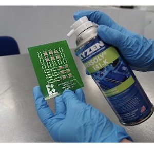
Cleaning No-clean Solder and Flux
December 31, 1969 |Estimated reading time: 7 minutes
Are no-clean soldering processes really more cost-effective or reliable enough for a given application? In situations where the product is mission-critical, will be conformally coated, has high operating voltages, among other scenarios, cleaning no-clean PCBs is necessary.
By Harald Wack, Ph.D., and Joachim Becht, Ph.D., Zestron
While most processes in the global electronics market are converging to use lead-free solder, the cleaning requirements, especially for no-clean flux formulations, have challenged traditional cleaning processes. This coincides with the continued miniaturization of assemblies and is compounded by an increased demand for cleanliness underneath low-stand-off components as un-cleaned or partially cleaned assemblies can lead to electrochemical failures in the field. Recent studies have been completed to address these emerging challenges with new chemical and mechanical product innovations.
Many manufacturers in the electronics industry have completed the conversion to no-clean solder pastes. No-clean solder pastes and fluxes are synthetic. As opposed to rosin-based and water-soluble fluxes, they offer a greater application range as well as many advantages with regard to performance. Although about 60% of the manufacturers using no-clean solder pastes can meet their customers' requirements without the additional step of cleaning residues, for the remaining 40%, perfect cleanliness is mission critical. Therefore, the term no-clean is really a misnomer, as many critical applications do require these pastes and fluxes to be cleaned.
Due to a rising number of current leakage and board reliability issues, particularly on coated assemblies, the electronics manufacturing industry has been experiencing an increased demand for substrate cleanliness. Studies have shown that conformal coating over contaminated PCBs may be a significant contributor to these failures. Similarly, the experts are vehemently concerned about the increasing operating voltages and, thus, long-term reliability of uncleaned, integrated electronic assemblies.

Figure 1. Encapsulation of organic activators.
Previously, low operating voltages (1–24 V) were not much of a concern as the electrical isolation between two contacts and/or components has been sufficient to prevent sparks. However, the integration of power supplies into assemblies caused an increase in voltages of up to 240 V. Furthermore, within the aviation and aerospace industries, electrical safety becomes even more of an issue as the higher ionic content of the atmosphere increases the flammability risk. Here, no-clean pastes have to be cleaned to eliminate any impact of their low-residue nature, according to J-STD-001, Class 3.1
Therefore, electrical safety is crucial, particularly when working in high-end and mission critical applications. This also raises the question about the ultimate cost effectiveness of so-called no-clean manufacturing processes compared to integrated cleaning processes.
The missing link between in-field failure rates and climatic and leakage current measurements of electronic assemblies has not yet been established. Actual weather conditions, unfortunately, cannot be simulated. The existing microclimate at the particular assembly location is strongly influenced by site-specific factors. The documentation of microclimatic conditions for electronic assemblies has only recently been possible, due to newly developed sensor technologies. And, such efforts have only been seen in sectors that have been affected by high failure rates such as the automotive industry. Consequently, there is a lack of available information at this time.
Studies on the long-term behavior of no-clean encapsulations show that the integrity of such film can easily be compromised (Figure 1). This phenomenon mainly depends on the quality of the encapsulation during the soldering step as well as on the degree of actual in-field temperature fluctuations (known as cycling). Some resin systems can also become brittle through simple oxidation reactions and therefore may ensure protection for only a limited period of time.
Several questions arise when examining the topics of full and partial encapsulation and the risks of no-clean solder and flux. With full encapsulation, can the reflow profile be 100% optimized? Is the inert resin layer exposed to climatic stress? With partial encapsulation, how much moisture will be absorbed by hygroscopic residues? In terms of electrical cleanliness, are leakage currents, corrosion, electrochemical migration, and bit failures of RF assemblies impedance-related?

HDI assemblies, particularly in the automotive industry, are more frequently used than ever. The sensitivity of these circuits to environmental interferences is accentuated by the use of high-resistivity components. High-frequency circuits between 30 MHz and 5 GHz are affected in particular. To maintain signal integrity, these systems not only require an adequate ohmic-insulation resistance; they must also have stable and complex impedance. The parasitic capacitances of contamination can distort the ramp up of the signal, thereby disrupting its integrity and leading to equipment malfunction.
Furthermore, reductions in SIR and the capacitive potential that can be built up by activator residues can be shown qualitatively under a scanning electron microscope (SEM). Imaging such contamination is possible by means of a test that responds selectively to carbon-acid-based activators. Another direct measurement to determine resistivity values (i.e., of remaining no-clean residues) can, for instance, be performed through impedance spectroscopy. This, in conjunction with other reliability tests, can determine the behavior of the assembly under appropriate climatic conditions to better assess the overall benefits that cleaning might have on a product.
Post-soldering process steps, such as the use of protective conformal coatings, should also be included into the discussion of clean vs. no-clean solder processes. Remaining no-clean residues on surfaces can, for instance, affect the degree of cross-linking. This may result in poor adhesion of protective coatings.2,3 During commissioned customer studies, delamination and electrochemical migration were documented underneath coatings with up to 0.4" thickness. The increasing bleed from within assemblies and components must also be considered. It can further limit the longterm adhesion of coatings and underfill materials. Unfortunately, these critical precipitations are generally <, hard to characterize or predict, and never monitored. Deteriorated signal integrity will therefore be neither explainable nor reproducible. As mentioned above, the no-clean process should ideally encapsulate all soils and residues to render them ineffective as causes of corrosion and current leakage.
The introduction of a cleaning process for the removal of no-clean flux residues clearly adds cost. Such expense, on the other hand, can be easily justified when compared to various current cost contributors of a no-clean process. For many electronic manufacturing companies, the consumption of nitrogen (even for the most modern oven systems) reflects one of the main consumable cost contributors to no-clean processes. It even exceeds solder paste as well as water usage. Due to generally higher soldering temperatures, nitrogen will be even less expendable, especially with regard to lead-free alloys.
Apart from pure cost and reliability considerations, other benefits clearly point towards implementing a proper cleaning process. An integrated cleaning process results in an overall improvement of adhesion of conformal coatings and a better ability to bond wire. For class 3 products, the J-STD 001D stipulates optical cleanliness (20–40×), as well as a rosin content of less than 258 µg/square inch and ionic contamination values of less than 10.06 µg/square inch.
Electronic components will continue to get smaller, board densities will increase, and assemblies will get even more difficult to clean. Recent studies have investigated the effectiveness of cleaning no-clean flux residues through chemical and mechanical adjustments, as well as the effects of temperatures above 160°F.4 Initial findings demonstrate that only marginal cleaning was achieved at belt speeds not commensurate with the demands of a production environment. After thorough analysis of the interaction between chemical and mechanical energy in the cleaning process, a new approach had to be evaluated to optimize pressure and flow mechanics. The impingement force of the cleaning agent had to be increased as the board is conveyed through the system. Various manifold designs, in conjunction with the latest cleaning agents, achieved the best results seen to-date in similar types of tests conducted over a period of years. The addition of one cleaning process step introduces further material/production flexibility, i.e., allowing use of more highly activated solder pastes and/or fluxes. Moreover, an adequate cleaning process could increase assembly process flexibility. Combining flux and alloy cleaning means users can include assemblies which, in the past, have been challenging to clean. Recently, the issue of cleanliness under low-standoff components for OA fluxes has emerged as DI-water is unable to fully remove all residues. Cleaning no-clean leaded and lead-free solder pastes in one single process is feasible without risk of cross contamination.5,7
Conclusion
Due to globalization, quality and reliability considerations are gaining prominence for domestic manufacturing companies. With more experience and knowledge, high-quality assembly producers are converting to chemistry-assisted cleaning processes. The overall benefit of cleaning can be realized by studying the positive effects on production quality and long-term climatic reliability. Due to the cited shortcomings of no-clean technologies, the debate of cleaning versus using a "no-clean" process results in one main conclusion: cleaning highly valuable and mission-critical electronic components is imperative and cost effective. SMT
REFERENCES:
- "Fluid Flow Mechanics: Key to Low Standoff Cleaning," IPC Midwest, 2008.
- "Reliable Coating with Proper Cleaning – Cleaning Process Benefits for EADS," Process Cleaning Magazine, January 2009.
- "Cleaning Lead-Free prior to Conformal Coating? Risks and Implications," APEX, 2006.
- "Thermal Residue Fingerprinting: A Revolutionary Approach to Develop a Selective Cleaning Solution," APEX, 2009.
- "Eutectic and Lead-Free Defluxing in One Single Process" SMT, March 2007.
- "Are lead-free assemblies specifically endangered by climatic safety?" APEX, 2004.
- "The Future of Cleaning OA Fluxes," SMT, September 2009.
Harald Wack, Ph.D., organic chemistry, president of ZESTRON Worldwide, mayb be contacted at h.wack@zestronusa.com. Joachim Becht, Ph.D., organic chemistry, is the head of R&D of ZESTRON Worldwide and may be contacted at j.becht@zestron.com.
More Surface Mount Technology Current Issue ArticlesMore Surface Mount Technology Archives Issue Articles
Share on:


