-

- News
- Books
Featured Books
- smt007 Magazine
Latest Issues
Current Issue
Intelligent Test and Inspection
Are you ready to explore the cutting-edge advancements shaping the electronics manufacturing industry? The May 2025 issue of SMT007 Magazine is packed with insights, innovations, and expert perspectives that you won’t want to miss.

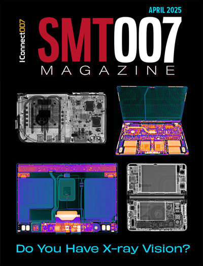
Do You Have X-ray Vision?
Has X-ray’s time finally come in electronics manufacturing? Join us in this issue of SMT007 Magazine, where we answer this question and others to bring more efficiency to your bottom line.

IPC APEX EXPO 2025: A Preview
It’s that time again. If you’re going to Anaheim for IPC APEX EXPO 2025, we’ll see you there. In the meantime, consider this issue of SMT007 Magazine to be your golden ticket to planning the show.
- Articles
- Columns
Search Console
- Links
- Media kit
||| MENU - smt007 Magazine
PCB Designer's Notebook
Planning for Very-fine-pitch and High IO Flip Chip: Part I of III
December 31, 1969 |
Estimated reading time: 6 minutes
In this three-part series, Vern Solberg will review flip chip packaging, the increased applications for flip chip in product design, and substrate and PCB design challenges for fine-pitch array-configured flip-chip applications. Part I explains how flip chips are created and how to work with these devices, small and large.
Although it has previously been regarded as a specialized application, flip-chip mounted semiconductors are gaining greater acceptance for achieving product miniaturization goals. Electronics companies continue their market strategy to provide greater product functionality in less space. To achieve these goals, the use of uncased die has become more commonplace. Although a wire-bond interface may remain the preference for many IC package applications, the direct face-down attachment interface of uncased die can significantly reduce the product’s form factor. Although area reduction plays a role in their decision to opt for flip-chip mounting, product developers also have realized that wire-bond interfaces cannot always meet optimum performance criteria for all applications, especially in higher-speed processor and ASIC products. For many of these newer generations of products, semiconductor suppliers have abandoned the traditional wire-bond package assembly methods altogether, opting instead for the more compact die face-down flip-chip attachment methodology. Although it is a common practice to mount the lower-I/O flip-chip die directly onto PCBs, placing a very-fine-pitch, high-pin-count die directly onto the host PCB may not be practical. Suppliers will generally rely on a slightly larger multilayer substrate interposer to enable more efficient circuit routing. The flip-chip-on-interposer package also allows the supplier to electrically test the device and, when needed, add a heat spreader to manage thermal dissipation conditions.
To accommodate flip-chip mounting, the die element requires a significant amount of preparation. The first consideration is the attachment method. The die can be furnished with a solid gold alloy contact using a conventional wire-bond system. The gold bump is ideal for gold-to-gold-interconnect (GGI) using ultrasonic bonding for interconnect; alternatively, the gold-bumped die can be efficiently mounted using an electrically conductive polymer material. The process that is of the greatest use, however, is solder bumping. The solder alloy material can be applied to the contact features with electroplating, stencil printing, or dispensing the specified alloy. The alloy traditionally adapted for flip-chip attachment was 90Pb/10Sn (90% lead). Due to material compatibility and various environmental concerns, alternative tin-based alloy compositions have become more common. To accommodate mounting flip-chip to an organic substrate material, users are favoring either a lower-melting-temperature eutectic composition or one of the lead-free alloys. When these alloys are heated to a liquidus state they naturally form an almost spherical bump profile.
The perimeter-bumped flip-chip process has historically served as the main interconnect method in direct-die attach packaging. Current generations of high-density wafer fabrication processes, however, are producing significantly smaller die in relationship to the number of contacts needed for electrical interface. The minimum perimeter contact pitch for flip chip generally ranges between 100 and 200 µm. From one generation to another, the die area may be reduced to increase the number of elements that can be furnished on a wafer. Due to the die-shrink factor, semiconductor makers may be forced to further reduce wire-bond area and pitch. It is not uncommon for these die elements to be furnished with bond site spacing significantly below 100 µm, which is not generally practical for solder bump attachment.
To overcome flip-chip mounting and circuit routing difficulties for the increased I/O semiconductors, companies have adopted a method for redistributing the contact locations over the active surface of the die using a rather complex wafer-level build-up fabrication process. Following a surface metallization process, copper circuit features are pattern plated onto a base metallization to provide narrow, solid copper conductors connecting the perimeter wire-bond features to contact sites arranged in a column- and row-configured array. After chemical ablation of the remaining base layer metallization, the copper conductors are over-coated with a photo-imaged dielectric material, leaving only the array of contact features exposed. Depending on die element complexity, as few as one and as many as four redistribution layers may be sequentially built up on the wafer surface. Because the contact sites remain free of the over-coating material, they can be prepped for the subsequent solder bumping process (typical of those noted above).
Several methods furnish solder-compatible contact features while the die elements remain in the wafer format. The most common and economical process simply deposits or electroplates a solder-compatible alloy at each contact site and, following surface heating, reflows the alloy to achieve a bond with the exposed copper contact sites. Preformed solder spheres may also be applied to the contact sites using a combination of flux coating, mass placement and reflow solder systems.
Preformed solder spheres provide a consistently uniform spacing at each contact site. Specialized systems have been developed to place the tiny alloy spheres individually or en masse. Sphere-to-contact joining occurs via either oven or laser reflow. Preformed spheres offer the advantage of maintaining a very repeatable stand-off dimension when the die is mounted onto the substrate. Uniform stand-off dimension enables access for post-assembly process flux residue removal via a cleaning step. This is a critical requirement for the larger die to accommodate underfill dispensing. Underfill is commonly applied to reinforce and physically stabilize the die-attach site. Having a residue-free surface allows unrestricted capillary flow of the liquid underfill material.
Another method for providing uniform contact profile on the die for solder mounting begins at the wafer fabrication stage. Fabs can apply a relatively thick temporary photo-resist material on the active surface of the die. After developing, only the contact site features are accessible for electroplating, furnishing raised and solid copper post-like features at each contact site.
Designing with Flip Chips
Uncased array-configured flip-chip die are no longer reserved for specialized low-volume electronics applications. Commercial wireless handsets (cell phones) manufactured in high-volume by one of the industry leaders, for example, use more than twenty 500-µm-pitch array-configured flip-chip semiconductor elements. These relatively low I/O devices (none greater in size than 5.0 mm2) are mounted on two sides of a conventional FR-4-based multi-layer substrate. Although a number of commercial low-I/O flip-chip die are available with contact spacing as wide as 400–500µm, the more advanced microprocessor and ASIC semiconductors will need to further reduce contact pitch because they may require that several thousand I/O contacts be confined in a very limited outline. A processor semiconductor product currently manufactured by a leading semiconductor company for high-end applications, for example, measures 18.0 × 20.0 mm. The die element is configured in the bumped array format, totaling 10,132 I/O. Typical of these high-end products, approximately half of the contacts are dedicated to power and ground distribution.
Designers will find that many die-level products are furnished with uniform array contact spacing; however, some die configured for flip-chip mounting may be furnished with two different contact pitch variations. The 10,000+ I/O semiconductor mentioned above, for example, is supplied with both 150 and 200 µm contact pitch for circuit routing efficiency. As the trend for greater semiconductor functionality continues, analysts expect high-performance Si-based product developers to expand the I/O requirement by 30% in the near future.
 Vern Solberg, an SMT Editorial Advisory Board Member, is a technical consultant specializing in surface mount and microelectronic design and development. Additionally, Vern holds several patents for IC packaging innovations and is a member of many industry organizations, including IPC, IMAPS, SMTA, and the JISSO International Council. He may be contacted at (408) 568-3734; vsolberg123@aol.com.
SMT, February 2010
In his next column, Part II of Planning for Very-fine-pitch and High I/O Flip Chip, Vern Solberg will address substrate and PCB design challenges for fine-pitch array-configured flip-chip applications. Read this column in the March/April issue of SMT.
Read More Columns from Solberg:Overcoming Imaging Challenges for High-density CircuitsPart 1: PCB Designer's Notebook: Fine-pitch and Die-size Array Packages Design and AssemblyPart 2: PCB Designer's Notebook: Stencil DesignPart 3: PCB Designer's Notebook: IC Component Package Evolution and the Impact of Lead-free SolderingPCB Designer's Notebook: Selecting Halogen-free (HF) Soldermask Materials


