-

- News
- Books
Featured Books
- smt007 Magazine
Latest Issues
Current Issue
Intelligent Test and Inspection
Are you ready to explore the cutting-edge advancements shaping the electronics manufacturing industry? The May 2025 issue of SMT007 Magazine is packed with insights, innovations, and expert perspectives that you won’t want to miss.

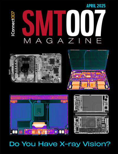
Do You Have X-ray Vision?
Has X-ray’s time finally come in electronics manufacturing? Join us in this issue of SMT007 Magazine, where we answer this question and others to bring more efficiency to your bottom line.

IPC APEX EXPO 2025: A Preview
It’s that time again. If you’re going to Anaheim for IPC APEX EXPO 2025, we’ll see you there. In the meantime, consider this issue of SMT007 Magazine to be your golden ticket to planning the show.
- Articles
- Columns
Search Console
- Links
- Media kit
||| MENU - smt007 Magazine
Intrusive Reflow of Lead-free Solder Paste, Part II
December 31, 1969 |Estimated reading time: 4 minutes
In SummaryIntrusive reflow describes the process of stencil printing solder paste in and around a thru-hole, placing SMT and thru-hole devices, then reflowing the entire assembly as part of the SMT process. This experiment is designed to determine the most effective parameters for successful reflow of acceptable lead-free thru-hole solder joints.
BY William E. Coleman, Photo Stencil; and George Oxx, Flextronics
Three stencil thicknesses (6, 8, and 15 mil), two board thicknesses (63 and 93 mil), and three thru-hole devices (resistor, DIP, and pin header) were specified in the design of experiment (DoE). Overprinting delivered sufficient solder paste to the thru-hole without use of a step stencil. Researchers determined that maximum wet-paste hole fill was achieved with a 45° blade angle, 0.5˝/sec. squeegee speed, and two strokes (i.e. a double print). Tin/silver/copper (SAC) paste was reflowed twice with components on the PCB, simulating assembly on a double-sided board. Researchers then studied resulting solder joints under high-magnification imaging and X-ray.
Test Results
Flux paste residue was measured for each stencil thickness and both board thicknesses. After reflow in a nitrogen atmosphere with less than 50-ppm oxygen, a large amount flux residue remained around the annular ring of the resistor and DIP thru-hole devices printed with a 6-mil-thick stencil on a 63-mil-thick board (Figures 1a and b), but good fillets formed for both devices. The stencil apertures were designed for 50% paste hole fill; however, 100% fill was achieved. Reducing the size of both overprint apertures for the resistor and DIP will reduce the paste volume, and thus flux residue, still leaving enough paste for a positive fillet. Redesigning the apertures should minimize the flux residue problem.
For the flux residue left on alternating headers printed with a 6-mil stencil/63-mil board, a smaller 57-mil annular ring (Figure 2a) exhibited higher levels of residual flux than a 66-mil annular ring (Figure 2b). The majority of 57-mil annular rings showed unacceptable excess flux levels. The 66-mil ring produced acceptable flux levels. With 15-mil-thick stencils, residual flux was too excessive. With a 93-mil-thick board, the 6-mil stencil provided acceptable flux residue amounts, while the 8-mil stencil was marginal and the 15-mil stencil created completely unacceptable results.
Header design - with a small hole and large annular ring - combined with a 6-mil-thick stencil provides acceptable levels of flux residue and satisfactory solder volume and fillets. Though the 6-mil-thick stencil created excess flux residues with the resistor and DIP, this can be controlled by redesigning the aperture sizes to print less solder paste.
 Figures 1A. Resistor and B. DIP printed with a 6-mil stencil.
Since the 6-mil-thick stencil provided acceptable flux-residue results for all three thru-hole devices, cross sections of samples printed with the 6-mil stencil then were examined for voiding and insufficient solder hole fill. Alternating headers with large annular rings showed mixed results. Generally, smaller holes showed less voiding and better fillets. For example, with a 63-mil-thick board, voiding occurred on 44- and 48-mil holes, but not on 36- or 40-mil locations. In the same situation on the thicker 93-mil board, 36- and 40-mil holes again showed minimal voiding. Negative fillets or unacceptable voiding turned up again in 44- and 48-mil holes. In smaller holes, fillets are higher on the 63-mil board compared to the 93-mil sample, but both are positive.
Wave vs. Intrusive Reflow
The main process-related issues with lead-free wave soldering of thru-hole devices include large voiding in the barrel, insufficient hole fill, and excessive flux residue buildup.
Electronics conversion to lead-free alloys creates several challenges for the wave solder process. These range from higher solder pot temperatures to extended preheat times/temperatures and difficult flux selection. Every parameter must be optimized to result in acceptable hole fill and minimal flux residue impacting ICT performance. OSP surface finishes add further complications to proper hole fill with wave soldering methods. This drives users to higher-solids fluxes, which then leave heavy residues on the board and wave pallets.
 Figures 2A. Alt. header with small annular ring and B. with large annular ring, both 6-mil stencil.
There are several advantages to implementing an intrusive reflow process. With high-temperature pin thru-hole (PTH) component materials required for lead-free, it’s possible to process some thru-hole devices in a full convection reflow furnace. This can eliminate manufacturing costs and issues associated with selective wave solder pallets; product handling during PTH component load; additional process steps and operators; quality hole fill; large voiding; additional copper dissolution of the barrels, due to slower conveyor speeds; and heavy wave solder flux residue buildup.
With proper setup of the intrusive reflow process, manufacturers can print a correct volume of solder paste into the hole and overprint on the top surface, reflowing a solder joint that meets industry standards (IPC-610-D) for hole fill. Using DfM information on pin-to-hole ratios, as identified in the experimental results, can further improve intrusive reflow products.
Conclusion
A DoE helped determine optimal paste hole fill for the printing process, leading to 100% hole fill for 63-mil-thick boards and 85% to 100% paste hole fill for the 93-mil-thick boards, dependant on hole size.
Testing performed with the three stencil thickness, two board thicknesses, and three thru-hole parts showed that a 6-mil stencil will provide good fillets without voiding or excess flux residue with proper design of the board’s barrel-hole dimension to pin dimension, aperture size, and print process setup. However, 8- and 15-mil stencils produce excess flux residue due to excess solder. Producing acceptable lead-free intrusive reflow results with a 6-mil stencil circumvents use of step stencils, or can make step stencil more workable in the process environment by reducing step depth. For example, 6-mil steps could be lessened to 5 mils.
ACKNOWLEDGEMENTS
“Stencil Design for Mixed-technology Thru-hole SMT Placement and Reflow,” William Coleman, Denis Jean, Julie Bradbury, SMT, July 2000.
To read Part I, see our November 2007 issue, archived on our Website at smtonline.com.
William E. Coleman, Photo Stencil; and George Oxx, Flextronics, may be contacted at bcoleman@photostencil.com; george.oxx@flextronics.com.


