


 Nolan's Notes: The Next Killer App in Component Manufacturing
 The Knowledge Base: Unlocking the Invisible—The Critical Role of X-ray Technology
 Standard of Excellence: Turning Negative Customer Feedback Into Positive Outcomes


Combining AOI and AXI: The Best of Both Worlds
December 31, 1969 |Estimated reading time: 6 minutes
AOI and AXI in a combined test platform ultimately will offer a faster return on investment (ROI) and improved yields.
By Claude LeBlond
Integration continues to flourish in the electronics sector. Each year, engineers integrate smaller, higher density chips and chip packages into their product designs to boost performance and further reduce the size of printed circuit board assemblies (PCBA). The relentless drive toward higher integration not only introduces new complications into the PCBA inspection process, but also motivates equipment manufacturers to introduce innovative new inspection systems designed to better meet today's rigorous inspection demands.
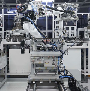
One such development is a combined vision, automated optical inspection (AOI) and automated X-ray inspection (AXI) system capable of detecting both visible and hidden defects from a single, integrated platform. An intelligently combined AOI/AXI test platform promises maximum test coverage in minimum space at a comparatively affordable price. In fact, an intelligently combined AOI/AXI system enables inspection professionals to leverage AOI's relative ease of use and fast set-up time to detect the majority of PCBA defects and then to leverage the more complex AXI capabilities for defects only visible via X-ray all without sacrificing throughput or time. As a result, an integrated system would give OEM and contract manufacturers (CM) the best of both worlds: AOI and AXI in a combined test platform that is physically smaller and less expensive to acquire and operate than two separate systems ultimately offering a faster ROI and improved yields.
Errors Increase When Complexity IncreasesBeyond the obvious cost and ease advantages, combined systems address a much more fundamental test and inspection issue: as board complexity increases, so does the incidence of errors both visible and hidden. For example, both human visual inspection and traditional in-circuit test (ICT) processes cannot keep pace with the increasing complexity of today's PCBAs. Today's smallest components, 0201s, are 0.020 x 0.010" (roughly the size of a fleck of pepper). At this miniscule size, human inspectors no longer can detect reliably if a component is slightly skewed or rotated, or if a solder joint is not perfect particularly at the speed necessary in a modern production environment. Additionally, today's complex packages may have as many as 200 to 300 individual connectors per package. This creates a dense line fan-out and decreases ICT access. As a result, in-line AOI systems are considered almost indispensable in today's production environment. As board complexity increases, however, AOI alone often is not enough. X-ray is the only technology capable of inspecting and reliably checking quality of hidden solder defects, such as voids, cold solder joints and poor solder adhesion. Only X-ray inspection can detect these problems effectively and monitor the quality process to provide the immediate feedback necessary for proactive process control.
Therefore, manufacturers increasingly must rely on both vision and X-ray capabilities. This makes an intelligently integrated combination system a potentially powerful tool for yield management.
AOI Systems 101 A key job for today's AOI system is to ensure that components are present and they remain in the correct location after reflow. Toward this end, AOI systems in their simplest form consist of one or more video cameras, lighting modules, and an image-processing computer. To compensate for the limited resolution of video cameras, the typical AOI system uses a combination of multiple cameras, switching among the cameras to inspect the PCBA. Cameras or scanners are the heart of the vision system and there are many variations on system approach and design. The number of cameras (or scanners) used depends on the pitch of the components being inspected small or large (Figure 1). Multiple cameras are sometimes necessary for multiple/variable component magnification.
 Figure 1. A fine-pitch quad flat pack is an example of the type of component pitch that optical inspection systems may use.
AOI systems are designed to locate component defects, including presence/absence, misalignment and polarity, then verify that the correct component is placed. AOI systems also can find very obvious or gross solder joint defects, e.g., shorts between leads, effectively.
Of particular note, the best of today's AOI systems are easy to program and use. Leveraging real-time learning software, some AOI systems eliminate the need for knowledge of image processing techniques or the use of complex rule-based algorithms reducing board programming time to just a couple of hours or less. With such systems, scanning example boards and allowing the software to generate features from the scanned images automatically can create inspection programs quickly and easily. The features are used by the software to develop a sophisticated model for each region of interest on the board. These AOI systems then can make intelligent decisions regarding component, lead and solder joint integrity, and the inspection programs continue becoming more robust through normal system operation.
AOI systems do have one significant shortcoming: they are not able to test devices with hidden solder connections, such as ball grid arrays (BGA) or chip scale packages (CSP), which are increasingly common in today's more sophisticated consumer, communications and other end products. The trend toward higher density, area-array packages and devices with hidden solder joints means that an AOI-only approach to in-line inspection often is no longer enough.
 Figure 2. An example of the type of solder defect that the AXI system can locate (open BGA). X-ray tests also can identify shorts, voids, misalignments and solder integrity.
X-ray Systems: The BasicsX-ray technology is the only way to ensure advanced PCBA integrity. Manual X-ray systems can verify the BGA manufacturing process prior to and during production. BGAs have very low parts per million (PPM) failure rates, so a sampling basis often can be used. However, BGAs do have defects, and thus many manufacturers require 100 percent testing of their BGA devices. Newer packaging technologies (CSPs, flip chips) are not as reliable as BGAs, so the use of AXI continues increasing. Generally, X-ray test is accepted as necessary for identifying shorts, voids, opens, misalignments and solder integrity of these new chip devices (Figure 2).
 Figure 3. AXI systems use an X-ray source to penetrate the target PCBA and to image the expected range of defect sizes. An X-ray-sensitive video camera converts the X-ray shadow of the PCBA into a video signal that then is enhanced and analyzed.
The typical X-ray system is a cabinet-type machine with lead-shielded walls and interlocked doors. The system includes an X-ray source of sufficient power to penetrate the target PCBA, and with satisfactory resolution to image the expected range of defect sizes. An X-ray-sensitive video camera converts the X-ray shadow of the PCBA into a video signal that then is enhanced and analyzed (Figure 3).
Optimally, AXI systems are designed to locate solder defects, including opens, shorts, and insufficient, excess and cold solder joints. AXI systems can find some component defects, such as missing and gross misalignments, but testing for component defects is an inherent weakness of AXI.
Of particular note, X-ray systems are difficult to program, requiring days or even weeks of setup time before they can inspect a new PCBA. This lengthy and complex programming cycle makes X-ray systems an impractical solution for short-run production.
An Integrated Combination An integrated in-line X-ray and vision system offers obvious advantages: by incorporating the best of today's AOI and AXI inspection capabilities into one in-line machine, a combination system provides a complete analysis without compromising line speed. Not only does the combination system allow manufacturers to inspect BGAs, flip chips and CSPs with hidden solder joints, but it also can inspect the PCBA assembly simultaneously for correct parts, position, orientation and other visual features. Additionally, by leveraging the intelligence and ease of use of today's most advanced vision systems, a combined approach offers fast setup, reduced need for complex AXI programming and a more complete defect detection solution. A comparison of AOI only, X-ray only and combined AOI/X-ray capabilities is shown in Table 1.

ConclusionToday, there are a proliferating number of automatic inspection systems in use by PCBA manufacturers. Given current market trends, it is fairly safe to state that today's PCBA producers require both AOI and X-ray inspection systems to ensure the highest quality and reliability of the boards shipped. For most production applications, a system using combination X-ray/vision technology means that manufacturers need only one machine to perform a thorough analysis of PCBAs for all component types.
Claude LeBlond, vice president of Engineering, may be contacted at Photon Dynamics, 125 Columbia, Aliso Viejo, CA 92656; (949) 448-0443; Fax: (949) 448-0445; E-mail: claude.leblonde@photondynamics.com; Web site: www.photondynamics.com.
Share on:


