-

- News
- Books
Featured Books
- smt007 Magazine
Latest Issues
Current Issue
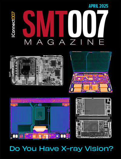
Do You Have X-ray Vision?
Has X-ray’s time finally come in electronics manufacturing? Join us in this issue of SMT007 Magazine, where we answer this question and others to bring more efficiency to your bottom line.

IPC APEX EXPO 2025: A Preview
It’s that time again. If you’re going to Anaheim for IPC APEX EXPO 2025, we’ll see you there. In the meantime, consider this issue of SMT007 Magazine to be your golden ticket to planning the show.

Technical Resources
Key industry organizations–all with knowledge sharing as a part of their mission–share their technical repositories in this issue of SMT007 Magazine. Where can you find information critical to your work? Odds are, right here.
- Articles
- Columns
Search Console
- Links
- Media kit
||| MENU - smt007 Magazine
Metal Stencil Overview
December 31, 1969 |Estimated reading time: 11 minutes
A definite learning curve exists when ordering the stencil for a printing process. When familiarization with its technologies helps produce desired results, the stencil becomes a constant in an otherwise variable assembly operation.
By Barry R. Goukler
"It takes a good stencil to get a good print, then automation helps make it repeatable."
Stencil acquisition is not only the first step in the assembly process, it is one of the most important. The primary function of the stencil is to facilitate solder paste deposition. The object is to transfer a precise amount of material to its exact location on the bare printed circuit board (PCB). The less paste hung up in the stencil, the more deposited on the board. Thus, when something goes wrong in the printing process, the first reaction is to blame the stencil. However, it is well to keep in mind that there are important variables other than those of the stencil that can affect its performance. These variables include the printer; particle size and viscosity of the solder paste; the style, material, durometer, speed and pressure of the squeegee blade; the breakaway of the stencil from the PCB (gasketing effect); thickness and flatness of the solder mask; and component planarity.
The TechnologiesThe three primary technologies for stencil manufacturing are chemical etching, laser cutting and electroforming. Each has distinct advantages and disadvantages. Chemical etching and laser cutting are subtractive processes; electroforming is an additive process. Accordingly, certain parameter comparisons, such as pricing, may fall into comparing apples to oranges. Instead, the main consideration should be performance coupled with cost and turnaround time.
Generally, chemically etched (chem-etched) stencils are just as effective as those of the other technologies when used for applications where the tightest pitch is 0.025" and over. Instead, laser-cut and electroformed stencils should be considered when dealing with 0.020" pitch and under. While the latter type stencils will work well for 0.025" pitch and over, it may be difficult to justify the cost and turnaround time.
 Figure 1. Etchant action is both vertical and horizontal in the creation of a knife edge, or hourglass, configuration.
Chem-etch StencilsChem-etch stencils are the workhorses of the stencil world. They are the most cost effective and the quickest to turn around. (Same day shipments are a daily occurrence.) Chem-etched stainless-steel stencils are created by coating a metal foil with resist, exposing an image onto both sides with a pin-registered phototool and then etching the foil from both sides simultaneously using a dual-sided process. Since the process is dual-sided, the apertures, or openings, are created as the etchant works through the metal not only from the top and bottom, but also horizontally. Inherent in this technique is the creation of a knife edge, or hourglass, configuration (Figure 1). While at 0.020" pitch and under, such a profile presents an opportunity for paste impedance, this drawback can be minimized with an enhancement process called electropolishing.
 Figure 2. The "smoothing" effect of electropolishing on the stencil's aperture walls significantly reduces surface friction and promotes good paste release.
Electropolishing is an electrolytic post process that "smooths" the aperture walls, resulting in reduced surface friction, good paste release and void reduction. It also can significantly reduce underside stencil cleaning. Electropolishing is achieved by attaching the foil to electrodes and immersing it in an acid bath. The electrical current causes the etchant to attack the rougher surface of the aperture first and to work harder on its walls than on the top and bottom surfaces of the foil, resulting in a "smoothing" effect (Figure 2). The foil then is removed before the etchant has an opportunity to attack top and bottom surfaces. Nevertheless, the latter surfaces are "polished" such that the solder paste will be rolled effectively (vs. being pushed) by the squeegee across the stencil surface and fill the aperture cavities.
Another technique to improve paste release for 0.020" pitch and under is trapezoidal section apertures (TSA).
 Figure 3. Trapezoidal section apertures, while promoting effective paste release, also form a "brick-like" deposit that assists firm component placement.
TSAs are openings that have a 0.001 to 0.002" larger dimension on the contact (or bottom) side of the stencil than on the squeegee (or top) side (Figure 3). The trapezoidal opening can be accomplished in two ways: by selectively modifying specific components, i.e., the contact-side dimension of the double-sided phototool is made larger than that of the squeegee side; or a stencil with global trapezoidal section apertures can be created by varying the top and bottom pressure settings of the etchant spray. The wall geometry, when smoothed by electropolishing, then permits paste release at 0.020" pitch and under. Additionally, the resulting solder deposit is in the form of a trapezoidal "brick," which promotes firm placement of the component and fewer bridgings.
 Figure 4. The stepdown feature (for variously pitched components) is recommended for at least 0.100" clearance between parts to permit complete paste distribution on both levels of the stencil.
Stepdowns, or dual-level stencils, can be produced easily via chem-etching techniques. This process reduces the solder volume for selected components by creating stepdown cavities. For example, with a large number of 0.050 and 0.025" pitch components (normally requiring a 0.007" thick stencil) in the same design with several 0.020" pitch quad flat packs (QFP), to reduce the solder paste volume deposited for the QFPs, the 0.007" thick stencil could be made with a stepdown area thickness of 0.005". The stepdown feature always will occur on the squeegee side of the mask since the contact side of the stencil must be level over the entire board (Figure 4). However, it is recommended that at least 0.100" clearance between the QFPs and the surrounding components be provided to permit the squeegee to completely distribute paste on both stencil levels.
 Figure 5. The electroforming process. The nickel atoms are deflected by the photoresist to create trapezoidal-shaped apertures.
Chem-etched stencils also do the best job of creating half-etched fiducials and title block nomenclature. Fiducials for alignment by printers with vision systems can be half-etched and then filled with a black epoxy to provide an easily recognizable contrast for the vision system to locate against a glossy metal background. Title blocks containing part number, creation date and other pertinent information also can be half-etched in the stencil for identification purposes. Both processes are accomplished by imaging only one-half of the double-sided phototool.
Chem-etch Limitations. In addition to the drawbacks of the knife-edge configuration, chem-etched stencils have another limitation: the aspect ratio. In simplest terms, the ratio limits the smallest aperture opening that can be etched in terms of the metal thickness at hand. Typically, for chem-etch stencils the aspect ratio is defined as 1.5 to 1. Thus, with a 0.006" thick stencil, the minimum aperture opening will be 0.009" (0.006" x 1.5 = 0.009"). By contrast, for electroformed and laser-cut stencils the aspect ratio is 1 to 1, i.e., one can create a 0.006" opening in a 0.006" thick stencil via either process.
ElectroformingAn additive rather than a subtractive process, electroforming creates a nickel stencil with a unique gasketing feature that reduces solder bridging and minimizes the need for underside stencil cleaning. This process provides near-perfect registration with no geometric limitations, smooth vertical sidewalls with a built-in taper and low surface tension to enhance paste release.
The stencil is created by imaging photoresist on a substrate (or mandrel) where the apertures are intended and then plating atom by atom, layer by layer the stencil around the resist to the desired thickness. As seen in Figure 5, the nickel atoms are deflected by the photoresist to create a trapezoidal configuration. Next, when the stencil is removed from the substrate, the top becomes the contact side to create the gasketing effect. A continuous nickel thickness range of 0.001 to 0.012" may be selected. This process is ideally suited for ultra-fine-pitch requirements (0.008 to 0.016") or for other applications. An aspect ratio of 1 to 1 can be achieved.
As for drawbacks, since a phototool is involved (albeit one-sided) the potential for misregistration exists. And if the plating process is not uniform, the gasketing effect is negated. Also, the gasketing "nubs" can be removed if the cleaning process is too vigorous.
Laser-cut StencilsProduced directly from the customer's original Gerber data, laser-cut stainless-steel stencils feature an absence of photographic steps. Hence, eliminating the opportunity for misregistration. A stencil can be made with excellent positional accuracy and reproducibility. The Gerber file, after the necessary modifications, is transferred to (and directly drives) the laser. Less physical intervention means fewer opportunities for error. Although there were initial concerns about the dross (vaporized molten metal) created by the laser beam, the current generation of laser cutters produces minimal dross that is removed easily.
 Figure 6. Pad geometries. With the transfer of Gerber data, pad configurations can be altered into various shapes as a means of reducing solder paste volume.
Concerns also have been raised over the aperture perimeter exhibiting a "scallop-like" outline with the resultant apertures having roughened walls. While this increases surface friction, the roughness is all in the vertical plane. However, late-generation laser machines have built-in vision systems, which allow for the foil to be cut in the unframed condition. This is significant because stencils can be produced by chem-etching the standard-pitch components and then laser-cutting the fine-pitch components. This "hybrid," or combination stencil, yields the benefits of both technologies at reduced cost and a quicker turn. Additionally, the entire stencil can be electropolished to provide smooth walls and excellent paste release. The major drawback of the laser-cut process is that the machine cuts each aperture individually. Naturally, the more apertures, the longer it takes and the more costly the stencil. However, if the design permits, cost can be reduced by taking advantage of the hybrid stencil process. Same day service is possible, depending on machine time availability. Trapezoidal apertures are created automatically per the laser beam's focus. The aperture openings actually are cut from the contact side of the stencil; the stencil then is flipped and mounted with the squeegee side up.
The laser technique is the only process that permits an existing stencil to be reworked, e.g., to add apertures, enlarge existing apertures or add fiducials.
Other AdvancesOther than laser cutting and electroforming, the most significant advance in stencil manufacturing has been electronic data transfer. As recently as 1995, the majority of artwork supplied to stencil manufacturers was in the form of film positives, which were expected to match the image on the bare copper 1 to 1. Component aperture modifications involved repetitive camera work and manual manipulations. The process also relied on the quality of the supplied film positive. Finally, the creation of step-and-repeat artwork was a tedious task.
 Figure 7. Adhesive conversion. With this capability, the solder paste layer in the design file can be converted to rounds and oblongs, depending on component size.
Today, electronic file transfer via modem and e-mail is the most common method of supplying image data instantaneously. Selective modifications, step-and-repeat images, and geometry conversions can be accomplished easily and accurately. Also, almost a full day can be cut off the turnaround time since the mailing of the film positive is eliminated.
With the transfer of Gerber files, pad geometries can be altered from squares and rectangles to "home plates," "grids," "zippers," etc. (Figure 6) as a means of reducing solder paste volume. Adjusting solder paste volumes by modifying geometries, combined with selecting the right metal thickness, also can eliminate the need for stepdowns. A single-level stencil, properly designed, is always better than a dual-level tool from a process standpoint.
Adhesive StencilsElectronic files also enable the computer-aided design (CAD) operator to easily determine the centroid of a pad configuration. With this capability, the solder paste layer in the design file can be converted to rounds and oblongs, depending on component size (Figure 7). Thus a stencil can be made, enabling one to "print," rather than dispense, adhesive. Printing is faster than dispensing, which frees up this equipment to work on other jobs.
Rework StencilsA more recent innovation occurs in the rework area. There are now "mini-micro" stencils available that are miniature stencils designed specifically to rework or repair individual components. Stencils may be purchased for single components such as standard QFPs and ball grid arrays (BGA). The mini-micro also comes with its own corresponding spatula, or mini-squeegee.
Pricing Comparisons
- Chem-etched stencil pricing is driven by the frame size. While the metal foil is the focus of the stencil creation process, the frame is the single, most expensive fixed cost. Its size is determined to a large extent by the type of printer. Most printers, however, will accommodate more than one frame size. (Frame sizes are industry standard.) Most stencil suppliers maintain an inventory of standard frame sizes ranging from 5 x 5" to 29 x 29". Since the blank metal foil cost is not as significant as that of the frame, metal thickness has no effect on pricing. And because all the apertures are etched simultaneously, their number also is of no consequence.
- Electroformed stencil pricing is driven primarily by the metal thickness (with an "adder" for whatever frame size is required). Plating up to the desired thickness is the dominant consideration: the thicker stencil costing more than the thinner.
- Laser-cut stencil pricing is according to the aperture number in the design.
The laser cuts each aperture one at a time, i.e., more apertures, the higher the cost. There also is an adder for the required frame size. A hybrid stencil where the laser cuts the fine-pitch and the standard-pitch components are chem-etched can be a cost effective method when many apertures are required. However, for designs having less than 2,500 apertures, it may be more cost effective to completely laser-cut the entire stencil.
SummaryWhatever current surface mount assembly needs may be, there presently is a stencil technology that meets that need. Some discussed innovations, such as trapezoidal section apertures, hybrid stencils and the pre-eminence of electronic data transfer, have all been developed and refined in the past three or four years. The stencil industry traditionally has been not only quick to respond to new requirements but also proactive in these ongoing developments.
This article is adapted from a presentation originally given at NEPCON West 2000.
REFERENCES
- C. L. Hutchins, "Fine-pitch Stencil Technology," SMT, July 1996.
- W. E. Coleman, "Stencil Design and Application for SMD, Through-hole, BGA and Flip Chips," Advancing Microelectronics, January/February 1996.
- R. Clouthier, "Appraising Stencils for Fine-pitch Printing," SMT, March 1995.
- W. E. Coleman, "Stencil Design for Advanced Packages," SMT, June 1996.
BARRY R. GOUKLER may be reached at Metal Etching Technology Associates Inc., #4 Lippincott Lane, Mt. Holly, NJ 08060; (609) 261-2670; Fax: (609) 261-4007; E-mail: sales@ metassocs.com; Web site: metassocs.com.


