-

- News
- Books
Featured Books
- smt007 Magazine
Latest Issues
Current Issue
Intelligent Test and Inspection
Are you ready to explore the cutting-edge advancements shaping the electronics manufacturing industry? The May 2025 issue of SMT007 Magazine is packed with insights, innovations, and expert perspectives that you won’t want to miss.

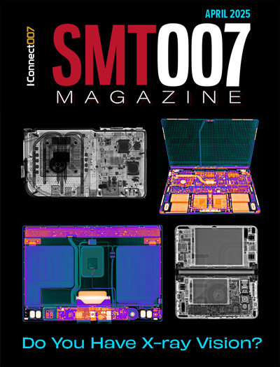
Do You Have X-ray Vision?
Has X-ray’s time finally come in electronics manufacturing? Join us in this issue of SMT007 Magazine, where we answer this question and others to bring more efficiency to your bottom line.

IPC APEX EXPO 2025: A Preview
It’s that time again. If you’re going to Anaheim for IPC APEX EXPO 2025, we’ll see you there. In the meantime, consider this issue of SMT007 Magazine to be your golden ticket to planning the show.
- Articles
- Columns
Search Console
- Links
- Media kit
||| MENU - smt007 Magazine
Rework Process for MicroBGA and CSP
December 31, 1969 |Estimated reading time: 9 minutes
By Thomas W. Dalrymple and Cynthia Milkovich
Reductions in package size and solder ball pitch with increased device density on PCBs lead to new assembly and rework challenges.
 Figure 1. Board pad layout for 144 I/O package.
As electronic assemblies become smaller, fine-pitch micro ball grid arrays (microBGA) and chip scale packages (CSP) meet the requirements for smaller, faster and higher performance electronic products. These low-cost packages can be found in many products such as laptop computers, cell phones and other portable devices. The reduction in package size and solder ball pitch with an increased device density on the printed circuit board (PCB) assembly causes new challenges to assembly and rework. Tight component spacings make component removal and replacement more difficult in a traditional hot-gas rework process without impacting nearby components. CSPs offer finer lead pitch that can present problems in site redressing and accurate component placement, and the lightweight, low-mass components risk misalignment and skewing as hot gas flows can displace the component. This article describes a process established on an automated hot-gas system for rework of several microBGA and CSP components. Reliability of reworked components and non-reworked components will be compared.
Process Verification
The objective of this project was to verify standard SMT assembly and rework processes for popular microBGA and CSP packages in the industry. Initial CSP assembly has become more prevalent in the industry but little work in component rework has been published. Board-level rework challenges because of small component size, reduced ball pitch and close proximity of other components require rework process development and optimization. Several components were chosen for this study (Table 1). The components represent various input/output (I/O) counts, pitches and package types.
Memory chip packages generally are low I/O packages such as packages 1, 2 and 4. It is not unusual for these packages to be used in double-sided or shared-via applications. Package 3, with 144 I/O, typically is used in a high-performance product application. All the CSPs attach with tin/lead (Sn/Pb) eutectic solder balls that range from 0.013 to 0.020". All the packages were stitched to allow for reliability testing.
Two test board designs were prepared for assembly. One design was a standard FR-4 PCB with surface wired or "dogbone" pad designs for wire escape. The second design used Surface Laminar Circuit (SLC) technology* and implemented captured photovias for wire escape rather than the dogbone design. The boards were 1 mm thick. Figure 1 shows a typical pad layout for the 144 I/O package.
Experimental Procedure
The rework process was performed on a hot gas rework tool** with a customized bias bay. This tool has the following capabilities:
- Hot-gas heating with a BGA nozzle
- Low air flow capability suitable for small microBGA and CSP rework
- Bottom board heating in custom bias bay
- Computer-controlled temperature profiles
- Calibrated vision system
- Automatic vacuum pickup and component placement.
The specific process flow followed is typical for BGA rework. The component is heated to solder reflow temperature with a hot-gas nozzle and then removed. Solder on the board site is removed with a solder vacuum tool until the site is planar. The site is then fluxed, a new component is aligned and placed, and solder is reflowed to attach to the board.

Thermal profiling is required for component removal and replacement. Profile parameters must match the solder paste manufacturer's recommended reflow temperatures and soaks. Each component site to be reworked is profiled individually, because of heat sinking variations of the board, internal layers and variations in adjacent components. In this manner, the risk of over- or under-heat exposure, or lifted pads, is minimized. Once profiles are achieved, the same conditions are used for all future reworks on the same sites. A separate process is developed for component removal and for component reflow attach, because of a modified reflow process. Figure 2 shows an example of a thermal profile using the rework tool's reduced flow rate capability (50 SCFH). Figure 3 shows a thermal profile for the larger components using a regular airflow setting (90 SCFH).
For component removal, the tool bias bay is set to 150°C to uniformly heat the board and minimize temperature gradients at the rework site. (Large temperature gradients can cause local board warpage.) The board is placed in a frame on alignment pins, supported 0.250" above the surface of the bay. Support blocks are taped to the backside of the board rework sites to prevent warpage during the heating process. The board is covered and preheated to a temperature of 135°C.
The rework tool uses a zero-force removal technique to remove the components from the board. When the process is started, the vacuum pick tube lowers to sense the height of the component, and then rises to a specific height for the heating sequence. When the component reaches reflow temperature, the vacuum pick lowers to the predetermined height, the vacuum turns on and the component is removed without collapsing the eutectic solder joints. The removed component is discarded and the board is heated for the next site removal.
 Figure 2. Reduced flow rate rework profile.
Site dress follows the component re-moval. This is accomplished using the automated solder scavenger on the rework tool. The board is placed in the bias bay and preheated to approximately 130°C. The rework site is fluxed*** prior to starting the process. The solder scavenger preheats to 420°C for SLC and 330°C for FR-4, checks for board height, and then moves across each row of pads with one pass, wicking solder up the vacuum tube as it moves along. Trial and error yield solder heights of 0.010" above the board's surface for the smaller component sites and 0.012" for the larger component sites. Sites are cleaned with isopropyl alcohol and inspected for damage. Typical observations to be avoided are solder smear and soldermask damage.
 Figure 3. Regular flow rate rework profile.
The component placement and reflow steps proceed as follows. The board is preheated to 135°C and the site is fluxed using a lint-free swab brushed across the board's surface. The flux serves to hold the component in place and to clean the pad surface prior to reflow. Component placement is achieved by aligning the component to the board using the rework tool's split optics capability.
Following component placement, the vacuum pick tube senses the height of the component and moves up a preset height. This allows the pick tube to remain in contact with the component within the hot-gas nozzle, keeping the component in place when the hot-gas preheat sequence begins. Following the preheat soak, the pick tube moves up an additional 0.015 or 0.020" to prevent component collapse during solder reflow.
Results and Discussion
Process adjustments were required for successful CSP component removal and replacement. At the peak temperature, the vacuum pick tube would lower to the component surface, collapsing the solder joints and splashing solder into the surrounding area on the board. Even though the rework tool reportedly used a zero-force removal technique, the slight pressure on the component was enough to collapse the small number of eutectic joints. The board also appeared to be warping upward, aggravating the condition. To prevent this, extra height was added to the removal sequence so the vacuum pick tube did not compress the joints during removal.
The automated site dress process successfully flattened the solder on the pads. This step is critical because the pads must be flat to prevent skewing during placement. The solder coating that remained typically was less than 0.001" tall on any of the pads. Figure 4 is an example of a typical site after removal and site dress.
 Figure 4. 46 I/O site after removal and site dress.
Component placement and reflow created the most difficulties. After fluxing the site, placing the component and reflowing the site, the components would often be skewed. On various occasions, the component balls did not wet even one pad on the board. It was believed that the components were too light and were moving around inside the hot-gas nozzle. This occurred even with the low airflow (50 SCFH) allowed by the rework tool. To prevent the components from moving, the rework tool was programmed to leave the vacuum pick tube in place on top of the component after placement and through the preheat portion of the thermal profile. The vacuum tube would retract slightly when the reflow cycle began, allowing the component to wet to the pads without collapsing the solder joints. This solution worked well, but it had some drawbacks. During reflow, the height and weight of the pick tube above the component would sometimes result in solder bridging. The vacuum pick tube also seemed to reduce the self-centering capability of the BGA.
 Figure 5. Cross-section of reworked CSP solder joint.
Another problem that surfaced was board warpage. Because the boards were quite thin, warpage was a great concern. Special support blocks were created to prevent warpage, and the board was preheated for each process to reduce temperature differentials that could cause warpage. Despite this, there were still problems. The board would bow lower under the pressure of a height reading, subsequently warping upward during a heating process. This meant that extra heights had to be added into each process to account for these differences. Even this was not enough. The same removal parameters would collapse one component in removal and yet not be close enough to remove another in the same location on another board.
Additionally, the board fluxing technique used was called into question; it was very subjective, varying greatly from one technician to the next. Too much flux created a liquid layer upon which the CSP components were able to float during reflow. At the same time, too little flux meant that there was nothing tacky keeping the component in place when the hot gas was first turned on. More recent work indicated that fluxing only the BGA joints themselves and not the board improved yields for the rework process. Final reworked solder joints had comparable joint structure to non-reworked solder joints as shown in Figure 5.
Reliability
Assembled test boards underwent accelerated temperature cycling (ATC) testing at -40° to 125°C and 0° to 100°C. Insulation resistance (IR) testing also was performed. No IR fails were found on any of the packages. Package 4 had early ATC fails (100 to 200 cycles, -40° to 125°C) and it was later discovered that the package supplier had discontinued this package because of reliability problems. Packages 1 through 3 performed well in 0° to 100°C testing (surviving greater than 1,000 cycles in most cases), while -40° to 125°C testing had mixed results. This temperature cycling range may have been too aggressive. Reworked components of packages 1 and 2 had slightly lower cycle life than non-reworked components, while package 3 had a comparable cycle life.
Conclusion
MicroBGA and CSP components can be reworked with a traditional hot-gas rework process. Rework process parameter adjustments are required to obtain a high yield. Because CSP components are small and lightweight, adjustments to hot-gas flow rate and vacuum pick tube height are required to avoid component misalignment or component collapse. Additional reliability testing of components reworked with an optimized rework process is warranted.
This article is adapted from a presentation originally given at APEX 2000.
*Surface Laminate Circuit (SLC) is a trademark of IBM Corp.** SRT Summit 2000.*** Senju SP 230C solder paste flux.
ACKNOWLEDGMENTS
The authors would like to thank Nadia Tonsi and supporters of this project. They also thank the APD lab team for building and reworking all test vehicles, particularly Craig Heim for his quality work and Lisa Jimarez for excellent rework support.
WORKS CONSULTED
- Irving Memis, "MicroBGA on Printed Wiring Boards: Recognizing the Need for Surface Laminar Circuit Microvia Wiring Capability," IBM, Endicott, N.Y.
- Alex Chen, et al., "Integrate CSP into Mainstream SMT Assembly Process," Advancing Microelectronics, IMAPS, Vol. 24, No. 6, p. 24-27.
- Reza Ghaffarian, Ph.D., "CSPs Assembly Reliability," Advancing Microelectronics, November/December 1997, p. 18-20.
THOMAS W. DALRYMPLE and CYNTHIA MILKOVICH may be contacted at IBM Microelectronics, Dept. U13G, Bldg. 002-2-B007, 1701 North St., Endicott, NY 13760; (607) 755-2671; Fax: (607) 755-8797; E-mail: twdalrym@us.ibm.com.


