


 Nolan's Notes: The Next Killer App in Component Manufacturing
 The Knowledge Base: Unlocking the Invisible—The Critical Role of X-ray Technology
 Standard of Excellence: Turning Negative Customer Feedback Into Positive Outcomes


Increased Yield and Reliability of the Flip Chip Process
December 31, 1969 |Estimated reading time: 13 minutes
By Brian J. Lewis
There are a number of process parameters that affect yield and reliability for flip chip assemblies. This article examines some of these parameters and discusses how examination of each parameter's role in the process, followed by necessary adjustments, can increase yield and reliability.*
 Figure 1. Yield offset for varying dip heights.
Although there are several processes in existence for mounting bare die on a printed circuit board (PCB), flip chip technology is unique in that the die is mounted active side down directly onto the substrate. Although some experimentation is being done with conductive adhesives, eutectic solder is commonly used for interconnection of the chip to the substrate.Solder is applied to the I/O on the chip, forming bumps of hardened solder. A requirement of the assembly process is to apply flux to the placement site prior to chip placement to facilitate reflow. The chip is placed on the substrate, and the solder bumps are aligned with contact pads on the substrate surface. This is followed by a solder reflow process that forms all the I/O connections simultaneously.One of the most critical aspects of the flip chip process is handling the stress between the chip and substrate because of dissimilar coefficients of thermal expansion (CTE). To compensate for the stress of thermal expansion, an underfill is applied in the standoff area between the substrate and chip. One of the biggest advantages of flip chip technology over other packaging and assembly techniques is the ability to support extremely high I/O counts. Because of the inherent higher yields of bare die processes, they are now preferred for chips with more than 200 I/O connections. Industry roadmaps are predicting that within the next three years, high-density flip chips will be capable of pitches less than 0.006" and more than 5,000 I/O. It is important to maximize the yield and reliability for the flip chip process.
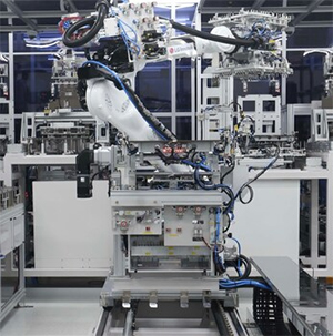
 Figure 2. Example of a low-cost flip chip process.
The Case Study Process for Parameter AnalysisBecause flip chip manufacturing processes can vary widely, affecting both the number and importance of certain parameters, a "starting point" from which to isolate and discuss the parameters that affect any of the processes needs to take place. A process design that "typifies" what is currently being utilized in this technology was sought for this study. The flip chip die used for this study measured 5 mm2 and had 88 I/O. The solder bumps were in a perimeter array and had a 200 μm pitch (center-to-center distance between the solder bumps). The eutectic solder bumps on the die were an alloy composition of 63 percent lead and 37 percent tin reflowed at 183°C. The boards were composed of standard high-temperature FR-4 material, with a Tg of 180°C. The pads on the substrate were composed of Cu/electroplated Ni/immersion Au metallurgy, and were defined by a 37.5 μm high soldermask layer. This soldermask defined the bond pad by blocking the trace material with a trench measuring 125 μm at the base and 185 μm at the top surface. The trench defined the top and bottom portions of the trace, and the sides of the trace confined the solder in the other direction. Substrate interconnections were daisy chained to probe points to provide two-point resistive continuity testing.The reflow oven was set up with a baseline profile developed for the boards being used. A standard baseline profile was implemented for the epoxy flux. This profile was set up using a thermal profiling unit. The forced-convection type oven used has five zones that were programmed with setpoints of 100°, 150°, 150°, 180° and 220°C. The zone temperature profile and the speed of the conveyor belt (20" per minute) gave a ramp rate of less than 3°C per second. When the boards were within 150° to 160°C, they soaked for 50 to 65 seconds. The boards were allowed to remain in the zone from 183°C to the peak temperature of 210°C for between 55 and 65 seconds. A placement machine** was used to pick the flip chip from a direct die feeder, dip the die bumps into an epoxy flux, place the die on the individual boards, and send the boards through the reflow oven. Next, a snap underfill pattern was applied to the chip, followed by underfill cure in an isothermal-zoned oven. A fast-flow, snap-cure, epoxy-based underfill material was used for the underfill process. The flow time was eight seconds per chip and the curing process required approximately five minutes.Controlled Variance of Process ParametersThe flux type, flux application, placement force and placement accuracy were the process variables of interest for this evaluation. Each of these parameters was varied to the process limits, and the resulting defects analyzed so a robust process window could be identified.Flux type. Most flux consists of a mixture of solvent, activator, and natural or modified resin. Chemically, the flux must remove oxides and contaminants from the surface of the solder bumps. The flux also allows for the transport of oxides and other reactive materials away from the areas to be soldered.
The choice of flux material is largely driven by the application method. The flux application method chosen for this application was a method of dipping the bumps of the flip chips into a controlled bath of medium-viscosity, epoxy-based flux. This dip-flux module is integrated into the placement machine, which minimizes process setup and maximizes efficiency and precision flux application. The dip module consists of a rotating disk that connected dip module. The disk spins while a "doctor's" blade skims below the surface of the flux, forming a thin flux layer for dipping. The type of flux used has a low solid content (around 3 percent) and is such that unwanted residues vaporize during the reflow process, eliminating the need for a secondary cleanup procedure.
Dip-flux height. This variable was looked at to see how a surplus or deficiency in flux would affect the solder wetting characteristics, the overall yield of the assemblies and the self-alignment characteristics of the solder bonding. Studied height adjustments varied from 25 to 45 to 65 μm. The change from the dip heights of 25 μm to the higher heights of 45 and 65 μm showed yield improvements of 15 percent. As for achieving the best yields, it was found that the 45 μm bath was the optimal height, with a 98 percent chip yield and 99.5 percent interconnect yield. Further calculations showed that the optimal dip height should be 35 to 45 percent of the solder bump height.
Dip time. When a dip-flux process is used, it is important to find the optimal time needed to allow the solder bumps to break the surface tension of the flux and for it to cover the solder bumps completely. This dip time was varied between 0.3 and 2.0 seconds. An optimal dip time for the die was approximately one second.
Dwell time. Given that flux is not as viscous as solder paste, there is always concern that the chip will slip on the board after placement. Dwelling (holding the chip at the placement site) will allow the flux to cure and increase in viscosity so it is better able to hold the chip in place. This dwell time observation was made to see if holding the chip to the board after fluxing increases yields. The same time range of 0.3 to 2.0 seconds that was used for dip time was used with this variable. Obviously, if dwell time is important and requires the upper end of the time range to optimize the yield, it can seriously affect throughput. The study showed that this variable had little affect on the overall yield.
No testing was carried out to determine dwell time requirements for "flux dispense" applications. However, if this had been a flux dispense application, the process would have had to allow enough dwell time for the flux to dry and become tacky. By allowing sufficient dwell time for a flux dispense application, most of the solvent in the flux mixture is given time to evaporate as the flux becomes more tacky. With less solvent present, there is less of a chance for the flux to boil off during reflow. By allowing sufficient dwell time, there is less chance that the chip will move prior to the solder bonding because the tackiness of the flux helps hold the chip in place.
Placement offset. In general, the industry requires that the die should be no more than 20 percent off the center of the pad. Most processes have tried to trim that down to 10 percent during optimal production speeds. In this experiment, the placement accuracy capability built into the placement machine was ignored (they were well within the 20 percent specs at optimal production rates); and the alignment was purposely offset as much as 55 percent. The actual offset placement settings varied from 0 to 55 percent.
The results of manipulating this variable were the most surprising. The study showed that self-alignment characteristics were strong enough to compensate for an offset of as much as 40 percent and still maintain optimal yield levels.
Figure 1 shows three charts that compare dipping height (25, 45 and 65 μm), plotting yield and offset percentage. This shows the overall effect of dip height on the self-alignment characteristic. As mentioned before, 45 μm was shown to be the optimal dip height.
Placement force. This parameter was varied from 100 to 500 g. It was found that this variable showed little effect on the overall yield for a chip having this relatively small I/O count (88 I/O). Although a force of around 500 g seemed to be optimal for the experimental chip, it is likely that chips with higher I/O density would require a higher placement force.
The Underfill ProcessGiven today's process alternatives, underfilling is a necessary part of every flip chip process. In terms of throughput, underfilling is the greatest bottleneck in the overall flip chip process. In fact, reducing the amount of time needed for dispensing the underfill, underfill flow and curing is perhaps the greatest challenge facing engineers in the surface mount industry. It is the roadblock that has kept the flip chip process from entering the ranks of mainstream SMT. Solving this problem deserves a sense of urgency, given the fact that current roadmaps call for a 30 to 40 percent growth for applications using flip chips during the next 10 years.
 Figure 3. Yield variable effects plot.
Giving full recognition to the importance of developing a fast and efficient underfill process, simultaneous experimentation is being conducted at the Manufacturing Research Center of the Georgia Institute of Technology. The experimentation design made use of much of what has been learned to date for improving the underfill process dynamics. A recent white paper written by Paul N. Houston, research engineer at Georgia Tech, describes a "low-cost" flip chip process ("Low-cost Flip Chip Processing and Reliability of Fast-flow, Snap-cure Underfills") that is shown in Figure 2. With a few exceptions, the experiment described in this article followed the same process flow. The experimental process did not use in-line dispensing equipment for the underfill. Instead, the underfill was applied and cured as a separate batch process. In contrast to the process shown in Figure 2, these were shortcuts that met the immediate needs of the experiment and do not reflect the recommended dynamics of an optimized process.
 Figure 4. Yield percentages at various thermal shock cycles.
In the study, an L-shaped underfill pattern of application was used. Dispensing the underfill with a 23-gauge needle of a liquid dispensing system,*** the line speed was 0.50" per second. Once the underside of the chip was filled, fillets were dispensed along other sides of the device. Getting the underfill completely under all areas of the die depends on capillary action, and the underfill experimentation being conducted at Georgia Tech has shown that this pattern of dispensing underfill presents the fewest number of voids. Georgia Tech uses acoustic microscopy to examine die underfill for voids.
The experiment took advantage of using the latest fast-flow, snap-cure underfill material currently available. Following the underfill material manufacturers' recommended temperature range and timing, the underfill was cured in a forced-convection oven. The total time required for curing was 5 minutes.
The study found that the reliability between the slow-cure, older-type underfill materials and the newer, snap-cure materials showed no difference. Choosing between a 1.5 hour cure vs. a 5 minute cure was an easy decision.
 Figure 5. High-throughput, "no-flow" flip chip assembly process.
ConclusionFigure 3 shows plot charts for all manipulated variables. As shown, the dipping time for the flux was the most significant.This study showed that placement accuracy for flip chips is not as critical as the industry has dictated. From a practical point of view, 20 percent offset will probably continue to be the minimal acceptable level. It is good to know that there is quite a bit of room for misalignment (as much as 40 percent) before it reaches a critical nature. This study shows 20 to 40 percent of this pad will ensure a robust process. The dip height for the fluxing plays a very significant role in overall yields. By increasing from a dip height of 25 μm to between 45 and 65 μm, the yield could be increased as much as 15 percent. Once the initial yield calculations and failure analysis were completed, the assembled boards were then subjected to thermal shock. The cycles were set at a temperature range of -55° to 125°C in accordance with MIL-Spec-883E at test condition B. Resistance and continuity testing was done at 100-cycle intervals. Once chip assemblies failed, scans were made using C-SAM and X-ray; the chip assemblies were then potted in a acrylic shell, preparing them for cross sectioning. As of 1,000 thermal cycles, there were no failures; the first failures did not occur until 1,100 cycles. The failures occurred in the 45 and 65 μm dip-height group. The first failure in the 25 μm group did not occur until the samples reached 1,400 thermal cycles, and by 1,800 cycles, only three of the die in the 25 μm group failed. Figure 4 shows thermal-cycling results.Although the 25 μm dip height seems optimal in regard to reliability, it was not the best choice for optimizing yield. But given the number of reliability failures vs. the lower yield data, the optimal dip height still appears to be 45 μm. Further analysis of the lower reliability numbers for this dip height is a subject for future testing.In SummaryAs the process for flip chips matures into the new millennium, the roles of some variables will certainly change. The results of this study reflect where the process is now. There is much to be solved and developed before flip chip technology can achieve full status as a high-volume, high-yield, low-cost surface mount solution. At the Manufacturing Research Center of Georgia Tech, several studies are currently being conducted that are focused on trying to improve the way in which the underfill is accomplished. One procedure being examined takes a completely different approach to the underfill process and its curing. A team under the direction of Professors Dan Baldwin and C.P. Wong has developed a material that acts as both a flux and an underfill. It is the heart of a flip chip process procedure known as "No-flow Underfill." The proposed process, shown in Figure 5, eliminates the intensive processes of dispensing and curing the underfill after the die is reflowed. The reflow oven has the dual role of forming the eutectic interconnections and curing the underfill with a single pass.
In whatever form the flip chip process eventually takes, one fact remains constant: Demand and production of subcompact products, as well as growing I/O counts, will continue to spiral upward. Flip chip assembly processes will meet the challenge and eventually enter the ranks of high-volume, cost-effective SMT.
- Siemens Energy & Automation partners with Georgia Institute of Technology on a broad range of flip chip technology studies, including the study on which this article is based.
** Siemens SIPLACE 80 F5.
*** CAM/ALOT 1818.
WORK CONSULTEDHouston, Paul, "Low-cost Flip Chip Processing and Reliability of Fast-flow, Snap-cure Underfills," Electronic Components and Technology Conference, p. 1310-19, June 1999.
BRIAN LEWIS is an advanced electronics packaging engineer with Siemens Energy & Automation Inc., Electronics Assembly Equipment, 2875 Northwoods Parkway, Norcross, GA 30071; (404) 894-6351; Fax: (404) 875-0668; E-mail: brian.lewis@eae.siemens.com.
Share on:


