-

- News
- Books
Featured Books
- smt007 Magazine
Latest Issues
Current Issue
Intelligent Test and Inspection
Are you ready to explore the cutting-edge advancements shaping the electronics manufacturing industry? The May 2025 issue of SMT007 Magazine is packed with insights, innovations, and expert perspectives that you won’t want to miss.

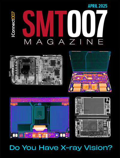
Do You Have X-ray Vision?
Has X-ray’s time finally come in electronics manufacturing? Join us in this issue of SMT007 Magazine, where we answer this question and others to bring more efficiency to your bottom line.

IPC APEX EXPO 2025: A Preview
It’s that time again. If you’re going to Anaheim for IPC APEX EXPO 2025, we’ll see you there. In the meantime, consider this issue of SMT007 Magazine to be your golden ticket to planning the show.
- Articles
- Columns
Search Console
- Links
- Media kit
||| MENU - smt007 Magazine
Conformal Coating Inspection: What Do You See?
March 27, 2013 |Estimated reading time: 9 minutes
Editor's Note: This article originally appeared in the February 2013 issue of SMT Magazine.
Inspection is a key aspect of the conformal coating application process and a successfully coated PCB.
Conformal Coating Standards
In today’s world of conformal coating processing, the main international standard used by most companies globally is IPC-A-610 Acceptability of Electronic Assemblies. The current version, IPC-A-610E, is available commercially from IPC. Other standards exist, including internal (company) standards, but this article focuses on the A610 for help in understanding the needs of conformal coating inspection.
IPC-A-610: Understanding the Issues
When looking at the IPC-A-610 standard, it should be considered section by section. This will make it easier to understand for both the needs of the operator and the conformal coating process itself. The standard is broken down into three sections: General, coverage, and coating thickness.
Conformal Coating: General
The IPC standard states that, in general, conformal coatings should be transparent, have a uniform colour and consistency, and cover the board and components uniformly. The coating coverage will depend on the application method.
From this there is much to infer, which can cause problems if interpreted incorrectly. Consider the fact that every conformal coating process is different--whether it is brush coating, robotic selective application using an airless valve, or spraying with an aerosol. All will produce different levels of finish and these finishes can vary depending on how the process is set up, which operator carries out the process, and the environment during production.
An interesting term used in the standard is “uniform.” Alone, the word could mean a great deal of things, but it must be taken in context with coverage details and thickness requirements discussed later. Ultimately, without them the term is of very little help.
The coating should be transparent. This calls into question the issue of using pigmented coatings and whether or not they are acceptable. This would be a customer query to be raised and the impact on the performance of the conformal coating should be assessed.
Conformal Coating: Coverage
Most conformal coatings now carry an optical brightener which, when exposed to ultraviolet (UV) light, fluoresces. This, in turn, allows easier inspection. However, some defects cannot be seen under UV and white (natural) light may also be needed. Some coatings have poor UV fluorescence due to the nature of the material. This can be seen in many silicone conformal coatings and can make inspection more difficult.
Whether or not the laminate or resist fluoresce at a similar level to the coating is also important--some conformal coating materials deliberately have no UV fluorescence because the optical brightener used has a detrimental impact on the coating and the PCB in the field.
In terms of coverage, the standard offers finish quality targets and different levels of quality: Class 1, 2, and 3. Targets include:
- No loss of adhesion.
- No voids or bubbles.
- No de-wetting, mealing, peeling, wrinkles, cracks, ripples, fisheyes, or orange peel.
- No embedded/entrapped foreign material.
- No discolouration or loss of transparency.
- Completely cure and uniform.
Achieving all of the above is virtually impossible for many conformal coating processes, circuit boards, and materials. To approach such a target consistently will, in general, be extremely costly in terms of money and investment and in process control time and effort.
Consider target of no bubbles. Even when using the naked eye to view the PCB it is normally impossible to not find bubbles anywhere on a circuit board, UNLESS:
- The conformal coating process is completely controlled.
- The material was selected correctly to achieve this result.
- The environment the process is in is completely optimised.
- The operators are fully trained to understand why the bubbles occur to control the process.
- The manufacturer of the PCB laminates, the assembly process, the components, or the conformal coatings do not change anything to cause an undesirable reaction.
Fortunately, approaching such targets is the desire, but not the necessity, for most companies. If it were necessity, conformal coating would be the exclusive realm of a few experts and unachievable by most. IPC helps here by offering acceptable criteria for the targets above.
IPC Acceptance Criteria for Conformal Coating
The IPC outline the acceptance criteria within the coverage section as being:
- Completely cured and homogeneous.
- Coating only in those areas where coating is required.
- Loss of adhesion adjacent to masking.
- No bridging of adjacent lands or conductive surfaces from:
- Loss of adhesion.
- Voids or bubbles.
- De-wetting.
- Cracks.
- Ripples.
- Fisheyes or orange peel.
- Foreign material does not violate minimum electrical clearance between components, lands, or conductive surfaces.
- Coating is thin, but still coats component/device edges.
These seem reasonable until you really consider what IPC is suggesting you attempt with your conformal coating process. You may realise your process or the process your customer requires is not as straightforward as it first appears.
First, consider having thin coverage on component/device edges. To achieve sharp edge coverage is an extremely tricky process and almost unachievable by most standard coating processes. It is quite difficult to actually tell if the sharp tips have coating using a normal inspection process. If a customer states that this is a requirement it must be considered very carefully.
Further, consider all the defects above and the requirement that there must be no bridging across conductive areas. This means that an operator must inspect EVERY spacing on a component populated PCB and ensure there are no defects like bubbles that cause a violation of this acceptance criteria. Not only is this an extremely skilled role to complete, but it is also extremely time consuming and may require an army of inspectors for high-volume work.
Before you agree to all acceptance criteria for conformal coating with a customer or your design engineer, considering exactly what you are agreeing to.
Conformal Coating Thickness
The final point addressed by IPC is conformal coating material thickness. The table in the standard gives the acceptable ranges for various resin materials such as acrylic conformal coating at 0.03 to 0.13 mm (30 to 130μm) when dried. This is a large range for application of conformal coating if all processes are set up correctly. It is also easy to be below or above this value if unaware of the fundamental issues. The key is to understand your conformal coating process and material capabilities.
For instance, using an automated dip coating system and achieving >30um dry film thickness with acrylic and polyurethane solvent-based coatings and avoiding all the defects in the acceptance criteria can be difficult to achieve. The coating tends to go on thinner than this and may not be thick enough to meet the criteria.
Further, a direct link exists between the number of bubbles preserved in a dried coating and the applied wet coating thickness for a single pass of coating. This is not difficult to understand: Put too much coating down in one go and the surface area cures (dries) before the bubbles in the body of the coating escape and they are trapped forever. Applying thin layers is critical to avoid bubbles. Yet, a selective robot normally applies only one coating. Therefore, there must be a trade-off and the application process must be fine-tuned to give optimum results.
If the coating is to be uniform, what does this really mean? Is this “uniform” within the range of 30 to 130um? Do you need to consider thin edge coverage where the coating pulls away from the sharp edges? Finally, as IPC points out, if the coating gathers under a device it is very easy to apply more than the 130um tolerance in certain areas. Unfortunately, contrary to natural thought, more is not better and should be avoided because, long term, the coatings may crack or craze if they are applied too thick.
Conformal Coating Automated Inspection Processes
As stated previously, meeting the acceptance criteria would require careful inspection of the entire PCB. Such inspection is an extremely difficult job due to factors such as eye strain, concentration drift, and throughput considerations. Can we not use automated conformal coating inspection?
The answer is “yes,” but with a few considerations and limitations.
Consider the conformal coating automated systems available. Some very sophisticated systems are now available with excellent camera or scanner technology, excellent software, and great process control. They can be either batch or inline and appear to be bridging the technology gap.
Camera systems can be fixed on three- and four-axis systems. Each camera will have to address parallax issues on 3D PCBs where there will be hidden areas down the sides of components. Scanner-based systems have the same parallax issues and parallax-free scanning systems are now available.
However, all these systems are somewhat flawed: They can look at all angles on every inch of the board, but still miss problem areas. But, this is not normally the critical factor with automated conformal coating inspection. Automated optical inspection (AOI) systems highlight the difficulty of the average conformal coating process to achieve IPC inspection acceptance criteria. AOI systems show the defects within the coating on the PCB and “see” more than an operator ever could.
This revelation can be like opening Pandora’s Box to the system user since now they can have a full line of PCBs with defects all over them. If this is the case, and the AOI system is set to inspect the conformal coat PCB using these rules, the production line will soon grind to a halt. Is this the fault of the AOI system? Is it the fault of the conformal coating process? Where does the fault lie?
The answer is simple: Most conformal coating processes are not producing the level of quality IPC inspection criteria desired. AOI systems see all defects (as long as mechanical and optical factors allow) very clearly. In fact, they see defects more clearly than the naked eye.
What is the Solution?
Create an investigative loop to develop the right solution.
- Determine what defects/inspection criteria are acceptable and define them.
- Determine what level of control and what defects can be generated through your current process or the new conformal process.
- If the system can achieve acceptance criteria everyone will be happy. If the process cannot meet acceptance criteria, change the criteria or the process.
Common sense is the ultimate solution and, with the right level of knowledge, the right solution is achievable. Finding the right inspection process will help you avoid excessive costs, arguments, and recriminations later on when problems arise.
 Dr. Lee Hitchens has worked in the conformal coating and reliability sector of the electronics industry for over 15 years and has considerable experience in all areas of reliability and conformal coating processing. He now divides his time between the roles of technical director of SCH Technologies in the UK, Diamond SCH in Shenzhen China, and Nexus3c, a Conformal Coating Centre, providing unique global services of independent consultancy, troubleshooting, and training in conformal coating and long-term reliability issues.


