


 Knocking Down the Bone Pile: Best Practices for Electronic Component Salvaging
 Global Citizenship: Together for a Perfect PCB Solution
 Smart Automation: Odd-form Assembly—Dedicated Insertion Equipment Matters


Henkel Leads Series C Investment in Vitriflex
June 4, 2015 | HenkelEstimated reading time: 1 minute
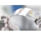
Based on the strong, continued progress in developing customized, integrated barrier films for display applications, The Electronics Group of Henkel has made an additional investment in ultra-barrier film technology innovator Vitriflex Inc. Henkel made its first equity investment and signed a joint development agreement (JDA) with the promising start-up company in May 2014. In this latest round, Henkel was the lead Series C investor.
“Combining Vitriflex’s expertise in ultra-barrier film innovation and Henkel’s leadership in adhesive technologies delivers a partnership that is advancing the state of the art of barrier film technology,” explains Mark Popovich, Henkel Corporate Vice President Global Marketing. “Since Henkel’s initial investment in Vitriflex, we have made profound progress toward an integrated barrier film product that delivers good adhesion to multiple substrates. This latest round of investment supports both the technology development work and the continued move toward high-volume manufacturing capability.”
Vitriflex, which was founded in 2010 and is run by a management and technical team that have extensive electronics market experience and barrier film expertise, has developed an ultra-barrier film technology that has low water vapor and oxygen transmission rates (WVTR and OTR) to meet the needs of emerging display technologies. Over the last year, Vitriflex technologists have worked in partnership with Henkel chemistry specialists to integrate optically transparent adhesives into ultra-barrier films with great success. Henkel’s additional investment in Vitriflex will progress this work, along with that of other applications.
“While the initial development priority was focused on flexible displays, our application scope and partnership with Henkel have expanded over the last year,” explains David Parker, Vitriflex President and CEO. “There are several other areas where we believe we can deliver differentiable technology value and we are pursuing those in earnest.”
The Series C investment furthers Vitriflex's move toward volume manufacturing capability to support multiple display technologies and sizes that range from handhelds to large-screen TV’s in excess of 100 inches. The company expects to have commercial product ready to ship at the end of 2015.
"Henkel intends to be a significant player in the display market," says Popovich in summary. "Our work with and investment in Vitriflex are significant components of Henkel’s broader display technology strategy."
About Henkel
Share on:


Testimonial
"We’re proud to call I-Connect007 a trusted partner. Their innovative approach and industry insight made our podcast collaboration a success by connecting us with the right audience and delivering real results."
Julia McCaffrey - NCAB GroupSuggested Items
Indium Corporation Earns Mexico Technology Award for New Halogen-Free Flux-Cored Wire
09/18/2025 | Indium CorporationIndium Corporation recently earned a Mexico Technology Award for its new high-reliability, halide- and halogen-free flux-cored wire, CW-807RS, which improves wetting speeds and cycle times for electronics assembly and robot soldering applications.
Blaize, Technology Control Company Partner to Power Saudi Arabia’s Next-Generation AI Innovation Infrastructure
09/17/2025 | BUSINESS WIREBlaize Holdings, Inc., a leader in programmable, energy-efficient edge AI computing, and Technology Control Company (TCC), a leading technology solutions provider in the Kingdom of Saudi Arabia (KSA), announced a strategic partnership to advance Saudi Arabia’s AI innovation infrastructure and accelerate its digital transformation goals.
BLT Joins Microchip Partner Program as Design Partner
09/17/2025 | BUSINESS WIREBLT, a U.S.-owned and operated engineering design services firm announced it has joined the Microchip Design Partner Program.
Curing and Verification in PCB Shadow Areas
09/17/2025 | Doug Katze, DymaxDesign engineers know a simple truth that often complicates electronics manufacturing: Light doesn’t go around corners. In densely populated PCBs, adhesives and coatings often fail to fully cure in shadowed regions created by tall ICs, connectors, relays, and tight housings.
On the Line With… Podcast: UHDI and RF Performance
09/17/2025 | I-Connect007I-Connect007 is excited to announce the release of a new episode in its latest On the Line with... podcast series, which shines a spotlight on one of the most important emerging innovations in electronics manufacturing: Ultra-High-Density Interconnect (UHDI).