


 American Made Advocacy: Smart Policies Can Ensure AI Data Centers Are Secure
 Beyond the Board: Early Engagement Means Faster Prototyping for Defense Programs
 Defense Speak Interpreted: The Autonomous Plane Battle—Skyborg Vs. Loyal Wingman


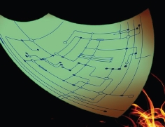
Flexible Circuit Materials for High-Temperature Applications
June 9, 2015 | Sidney Cox, DuPont Circuit and Packaging MaterialsEstimated reading time: 1 minute
Abstract
Many opportunities exist for flexible circuits in high-temperature applications (automotive, military, aerospace, oil and gas). Flex circuits in these applications have been hindered by a lack of materials that can survive higher temperatures. Some materials, especially some thermoset adhesives, break down over time at higher temperature, becoming brittle or losing adhesion to copper. Polyimides tend to perform much better under high temperature.
The other issue is the lack of good test methods to verify that flex materials can survive higher temperatures. Several methods for testing copper clad laminates exist, but there are very few for coverlays and bondplies. We will discuss different test methods for measuring high-temperature capability including the new IPC service temperature test. We will also report on test results for various flexible materials and our recommendations for the best flexible materials for high temperature applications. This will include development work on new flex materials for high-temperature applications.
Introduction
More applications require flexible circuits that must survive high-temperature environments. These include automotive applications near the engine, oil and gas down-hole pumps, and aerospace applications near jet engines. There have been limited test methods to determine what temperatures flexible materials can survive.
The damage caused by high-temperature environments will mainly fall in three categories: loss of adhesion between copper and dielectric, loss of adhesion between dielectric layers, and embrittlement of the dielectric layers. At the highest temperatures the copper would also become brittle, but in most cases the flexible circuit dielectrics fail first. Thermoset adhesives seem to be most sensitive to embrittlement especially compared to polyimide films which are much more resistant to high temperatures.
Read the full article here.
Editor's Note: This article originally appeared in the June 2015 issue of The PCB Magazine.
Share on:


Testimonial
"In a year when every marketing dollar mattered, I chose to keep I-Connect007 in our 2025 plan. Their commitment to high-quality, insightful content aligns with Koh Young’s values and helps readers navigate a changing industry. "
Brent Fischthal - Koh YoungSuggested Items
WestDev Announces Advanced Thermal Analysis Integration for Pulsonix PCB Design Suite
10/29/2025 | WestDev Ltd.Pulsonix, the industry-leading PCB design software from WestDev Ltd., announced a major enhancement to its design ecosystem: a direct interface between Pulsonix and ADAM Research's TRM (Thermal Risk Management) analysis software.
Designers Notebook: Power and Ground Distribution Basics
10/29/2025 | Vern Solberg -- Column: Designer's NotebookThe principal objectives to be established during the planning stage are to define the interrelationship between all component elements and confirm that there is sufficient surface area for placement, the space needed to ensure efficient circuit interconnect, and to accommodate adequate power and ground distribution.
Episode 6 of Ultra HDI Podcast Series Explores Copper-filled Microvias in Advanced PCB Design and Fabrication
10/15/2025 | I-Connect007I-Connect007 has released Episode 6 of its acclaimed On the Line with... American Standard Circuits: Ultra High Density Interconnect (UHDI) podcast series. In this episode, “Copper Filling of Vias,” host Nolan Johnson once again welcomes John Johnson, Director of Quality and Advanced Technology at American Standard Circuits, for a deep dive into the pros and cons of copper plating microvias—from both the fabricator’s and designer’s perspectives.
Nolan’s Notes: Tariffs, Technologies, and Optimization
10/01/2025 | Nolan Johnson -- Column: Nolan's NotesLast month, SMT007 Magazine spotlighted India, and boy, did we pick a good time to do so. Tariff and trade news involving India was breaking like a storm surge. The U.S. tariffs shifted India from one of the most favorable trade agreements to the least favorable. Electronics continue to be exempt for the time being, but lest you think that we’re free and clear because we manufacture electronics, steel and aluminum are specifically called out at the 50% tariff levels.
MacDermid Alpha & Graphic PLC Lead UK’s First Horizontal Electroless Copper Installation
09/30/2025 | MacDermid Alpha & Graphic PLCMacDermid Alpha Electronics Solutions, a leading supplier of integrated materials and chemistries to the electronics industry, is proud to support Graphic PLC, a Somacis company, with the installation of the first horizontal electroless copper metallization process in the UK.