-

-
News
News Highlights
- Books
Featured Books
- smt007 Magazine
Latest Issues
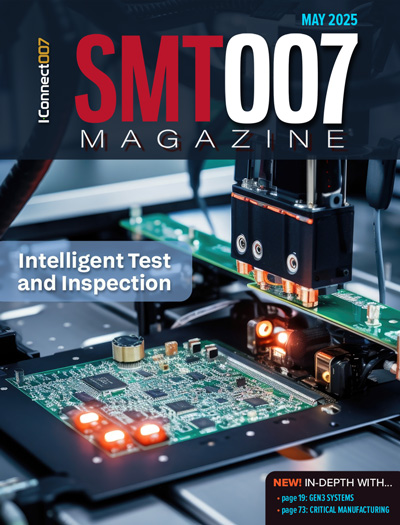
Current Issue
Moving Forward With Confidence
In this issue, we focus on sales and quoting, workforce training, new IPC leadership in the U.S. and Canada, the effects of tariffs, CFX standards, and much more—all designed to provide perspective as you move through the cloud bank of today's shifting economic market.

Intelligent Test and Inspection
Are you ready to explore the cutting-edge advancements shaping the electronics manufacturing industry? The May 2025 issue of SMT007 Magazine is packed with insights, innovations, and expert perspectives that you won’t want to miss.

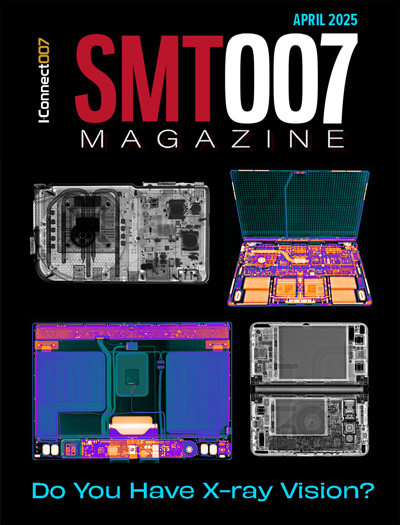
Do You Have X-ray Vision?
Has X-ray’s time finally come in electronics manufacturing? Join us in this issue of SMT007 Magazine, where we answer this question and others to bring more efficiency to your bottom line.
- Articles
- Columns
Search Console
- Links
- Media kit
||| MENU - smt007 Magazine
The War on Soldering Defects under Area Array Packages: Head-in-Pillow and Non-Wet Open
August 17, 2015 | Jason Fullerton, AlphaEstimated reading time: 2 minutes
The most difficult aspect of any soldering defect on an area array package is the inability to observe the defect easily. It is important to understand the characteristics of soldering defects in order to identify the proper action to take to mitigate the defects in a soldering process.
Head-in-pillow (HiP) defects are soldering defects on area array packages characterized by a lack of coalescence between the solder paste deposit and the package solder bump. In these defects, the solder paste deposit coalesces properly with itself and typically wets to the PCB land. Displacement of each solder deposit (paste and bump) is a common feature of HiP defects.
Non-wet open (NWO) defects are soldering defects characterized by a lack of wetting to a PCB land by a fully coalesced solder deposit on an area array package. In this defect, the solder paste and the package solder bump coalesce together fully without wetting to the PCB land.
A spherical or nearly spherical shape along the PCB side of the bump is a common feature of NWO defects.
What Head-in-Pillow and Non-Wet Open are not
It is important to discuss defects that can share some symptoms with HiP and NWO, in order to contrast against defects that require different mitigation actions. One example of a defect with similar symptoms to HiP and NWO is insufficient solder paste volume transfer during printing. In this case, it can appear that no wetting has occurred to the land and mimic NWO (especially if no paste has been transferred). If a small amount of paste has been printed, the resulting connection can initially appear to be consistent with HiP. Troubleshooting of HiP and NWO defects should include steps to ensure the solder paste printing process is properly controlled and performing well.
Another defect that can be confused with HiP is cold solder, which is characterized by a lack of coalescence of the solder paste deposit. HiP is a defect that occurs in the presence of a well-defined and controlled reflow process, which ensures coalescence of the solder paste deposit. Diagnosis of a defect as HiP should include an examination of the reflow profile to ensure that the process is not at risk of causing the occurrence of cold solder.
Non-wetting to a PCB land has many causes that should be familiar to most with experience troubleshooting solder defects. These defects can easily be confused with NWO since both defects share a symptom: poor wetting of a coalesced solder bump to the PCB land. The key difference is that NWO defects result in a solder bump that is spherical along the PCB side. A defect that is solely caused by poor PCB solderability will generally demonstrate the same shape as a typical area array solder connection: flatter and wider than a sphere and generally sharing the contour of the land along that interface. Testing the solderability of the PCB lands is an important step when attempting to determine if a wetting defect is a result of NWO defects.
Editor's Note: This article originally appeared in the August 2015 issue of SMT Magazine.
Suggested Items
See TopLine’s Next Gen Braided Solder Column Technology at SPACE TECH EXPO 2025
05/28/2025 | TopLineAerospace and Defense applications in demanding environments have a solution now in TopLine’s Braided Solder Columns, which can withstand the rigors of deep space cold and cryogenic environments.
INEMI Interim Report: Interconnection Modeling and Simulation Results for Low-Temp Materials in First-Level Interconnect
05/30/2025 | iNEMIOne of the greatest challenges of integrating different types of silicon, memory, and other extended processing units (XPUs) in a single package is in attaching these various types of chips in a reliable way.
E-tronix Announces Upcoming Webinar with ELMOTEC: Optimizing Soldering Quality and Efficiency with Robotic Automation
05/30/2025 | E-tronixE-tronix, a Stromberg Company, is excited to host an informative webinar presented by Raphael Luchs, CEO of ELMOTEC, titled "Optimize Soldering Quality and Efficiency with Robotic Automation," taking place on Wednesday, June 4, 2025 at 12:00 PM CDT.
CE3S Launches EcoClaim Solutions to Simplify Recycling and Promote Sustainable Manufacturing
05/29/2025 | CE3SCumberland Electronics Strategic Supply Solutions (CE3S), your strategic sourcing, professional solutions and distribution partner, is proud to announce the official launch of EcoClaim™ Solutions, a comprehensive recycling program designed to make responsible disposal of materials easier, more efficient, and more accessible for manufacturers.
Indium to Feature Precision Gold-Based Die-Attach Preforms at IMS 2025
05/29/2025 | Indium CorporationIndium Corporation® will feature its high-reliability, gold-based precision die-attach preforms for critical laser and RF applications, as well as 5G communications, at the International Microwave Symposium, June 15-19, in San Francisco, CA.


