


 It’s Only Common Sense: Marketing Isn’t Fluff, It’s Ammunition
 Driving Innovation: Mechanical and Optical Processes During Rigid-flex Production
 The Chemical Connection: Onshoring PCB Production—Daunting but Certainly Possible


Characterization of PCB Material & Manufacturing Technology for High-Frequency
September 2, 2015 | E. Schlaffer, AT&S; and O. Huber, T. Faseth, and H. Arthaber, University of Technology, ViennaEstimated reading time: 15 minutes
Abstract
Today's electronics industry is changing at a rapid pace. The root causes are manifold. The world population is growing toward eight billion, which gives rise to new challenges in terms of urbanization, mobility and connectivity. Consequently, numerous new business models for the electronic industry will develop. Connectivity will influence our lives more than ever. Concepts like Industry 4.0, Internet of Things, M2M communication, smart homes and communication in, or to cars are maturing. All these applications are based on the same demanding requirement—a considerable amount of data and increased data transfer rate. These arguments present major challenges to PCB design and manufacturing.
This paper investigates the impact of different PCB manufacturing technologies and their relation to high-frequency behavior. In the course of the paper a brief overview of PCB manufacturing capabilities will be presented. Moreover, signal losses in terms of frequency, design, manufacturing processes, and substrate materials are investigated. The aim of this paper is to develop a concept to use materials in combination with optimized PCB manufacturing processes, which allows a significant reduction of losses and increased signal quality.
First analysis demonstrates that for increased signal frequency, demanded by growing data transfer rate, the capabilities to manufacture high-frequency PCBs become a key factor in terms of losses. Base materials with particularly high-speed properties like very low dielectric constants are used for efficient design of high-speed data link lines. Furthermore, copper foils with very low treatment are to be used to minimize loss caused by the skin effect. In addition to the materials composition, the design of high-speed circuits is optimized with the help of comprehensive simulation studies.
The work on this paper focuses on requirements and main questions arising during the PCB manufacturing process in order to improve the system in terms of losses. For that matter, there are several approaches that can be used. For example, the optimization of the structuring process, the use of efficient interconnection capabilities, and dedicated surface finishing can be used to reduce losses and preserve signal integrity.
In this study, a comparison of different PCB manufacturing processes by using measurement results of demonstrators that imitate real PCB applications will be discussed. Special attention will be drawn to the manufacturing capabilities that are optimized for high-frequency requirements and focused to avoid signal loss. Different line structures like microstrip lines, coplanar waveguides, and surface integrated waveguides are used for this assessment.
This research was carried out by Austria Technologie & Systemtechnik AG (AT&S AG), in cooperation with Vienna University of Technology, Institute of Electrodynamics, Microwave and Circuit Engineering.
Introduction
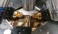
Several commercially available PCB fabrication processes exist for manufacturing PCBs. In this paper two methods, pattern plating and panel plating, were utilized for manufacturing the test samples.
The first step in both described manufacturing processes is drilling, which allows connections between different copper layers. The second step for pattern plating (see figure 1) is the flash copper plating process, wherein only a thin copper skin (flash copper) is plated into the drilled holes and over the entire surface. On top of the plated copper a layer of photosensitive etch resist is laminated which is subsequently imaged by ultraviolet (UV) light using a negative film. Negative film imaging is exposing the gaps in between the traces to the UV light. In developing process the non-exposed dry film is removed with a sodium solution. After that, the whole surrounding space is plated with copper and eventually covered by tin. The tin layer protects the actual circuit pattern during etching. The pattern plating process shows typically a smaller line-width tolerance, compared to panel plating, because of a lower copper thickness before etching. The overall process tolerance for narrow dimensions in the order of several tenths of µm is approximately ± 10%.
Figure 1 (left) - Pattern plating; Figure 2 (right) - panel plating.
The second typical PCB manufacturing process is panel plating (see Figure 2). In this process, after drilling, the entire panel is plated with copper. On top of the plated copper a layer of photosensitive etch resist is laminated. After that, there is positive film imaging, whereby the actual circuit pattern is exposed to UV light. After developing, the copper is etched with a chemical wet process and in the last step the etch resist is removed and the copper structure is finished. It should be noted that in panel plating the etching is applied on the whole thickness of plated copper and copper foil. During panel plating the copper thickness varies up to ± 3% only, because of the uniform plating method. However, the distribution of the etching solution on the surface is unequal; a lower exchange of etching solution and copper occurs in the center and somewhat more on the edges of a production panel. This is called “puddling effect.” The consequences are wider lines in the center and narrower lines at the edges of each panel. The overall process tolerance for narrow dimensions in the order of several tenths of µm is approximately ± 20%.
Page 1 of 5
Share on:


Testimonial
"We’re proud to call I-Connect007 a trusted partner. Their innovative approach and industry insight made our podcast collaboration a success by connecting us with the right audience and delivering real results."
Julia McCaffrey - NCAB GroupSuggested Items
WestDev Announces Advanced Thermal Analysis Integration for Pulsonix PCB Design Suite
10/29/2025 | WestDev Ltd.Pulsonix, the industry-leading PCB design software from WestDev Ltd., announced a major enhancement to its design ecosystem: a direct interface between Pulsonix and ADAM Research's TRM (Thermal Risk Management) analysis software.
Designers Notebook: Power and Ground Distribution Basics
10/29/2025 | Vern Solberg -- Column: Designer's NotebookThe principal objectives to be established during the planning stage are to define the interrelationship between all component elements and confirm that there is sufficient surface area for placement, the space needed to ensure efficient circuit interconnect, and to accommodate adequate power and ground distribution.
Episode 6 of Ultra HDI Podcast Series Explores Copper-filled Microvias in Advanced PCB Design and Fabrication
10/15/2025 | I-Connect007I-Connect007 has released Episode 6 of its acclaimed On the Line with... American Standard Circuits: Ultra High Density Interconnect (UHDI) podcast series. In this episode, “Copper Filling of Vias,” host Nolan Johnson once again welcomes John Johnson, Director of Quality and Advanced Technology at American Standard Circuits, for a deep dive into the pros and cons of copper plating microvias—from both the fabricator’s and designer’s perspectives.
Nolan’s Notes: Tariffs, Technologies, and Optimization
10/01/2025 | Nolan Johnson -- Column: Nolan's NotesLast month, SMT007 Magazine spotlighted India, and boy, did we pick a good time to do so. Tariff and trade news involving India was breaking like a storm surge. The U.S. tariffs shifted India from one of the most favorable trade agreements to the least favorable. Electronics continue to be exempt for the time being, but lest you think that we’re free and clear because we manufacture electronics, steel and aluminum are specifically called out at the 50% tariff levels.
MacDermid Alpha & Graphic PLC Lead UK’s First Horizontal Electroless Copper Installation
09/30/2025 | MacDermid Alpha & Graphic PLCMacDermid Alpha Electronics Solutions, a leading supplier of integrated materials and chemistries to the electronics industry, is proud to support Graphic PLC, a Somacis company, with the installation of the first horizontal electroless copper metallization process in the UK.