-

- News
- Books
Featured Books
- design007 Magazine
Latest Issues
Current Issue
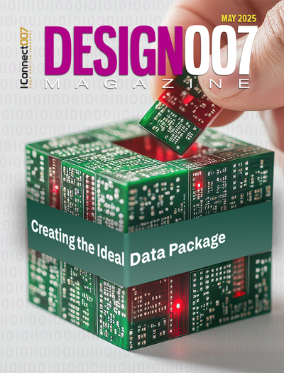
Creating the Ideal Data Package
Why is it so difficult to create the ideal data package? Many of these simple errors can be alleviated by paying attention to detail—and knowing what issues to look out for. So, this month, our experts weigh in on the best practices for creating the ideal design data package for your design.

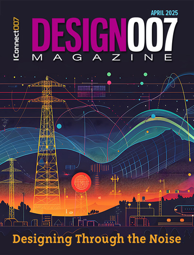
Designing Through the Noise
Our experts discuss the constantly evolving world of RF design, including the many tradeoffs, material considerations, and design tips and techniques that designers and design engineers need to know to succeed in this high-frequency realm.

Learning to Speak ‘Fab’
Our expert contributors clear up many of the miscommunication problems between PCB designers and their fab and assembly stakeholders. As you will see, a little extra planning early in the design cycle can go a long way toward maintaining open lines of communication with the fab and assembly folks.
- Articles
- Columns
Search Console
- Links
- Media kit
||| MENU - design007 Magazine
Accelerating the Design Cycle : Moving from Discipline-Centric to Product-Centric Design
October 28, 2015 | Bob Potock, ZukenEstimated reading time: 2 minutes
Defining the characteristics of a new product, such as features, size, weight, and battery life, is the job of marketing. Realizing those design requirements is the responsibility of a multidisciplinary team consisting of product architects, hardware engineers, software engineers, mechanical engineers, packaging engineering, manufacturing engineers, purchasers, etc.
Today, the design process in most cases fans out from the requirements as defined by marketing into multiple independent design threads that converge at the prototype. There is usually no systematic method for these different disciplines to communicate their work to the other disciplines. This lack of communication often leads to conflicting design decisions, such as when an electrical engineer or purchaser selects a component without having any way of knowing that it interferes with the enclosure. Extra design turns are often needed to resolve these conflicts at the prototype stage.
This obstacle, and many others, can be overcome by a product-centric design process that enables all disciplines to work collaboratively during a new virtual prototyping and detailed design. During the architectural validation or virtual prototyping phase, each contributor can optimize the design from their own perspective with visibility and change notices from the others. The product optimization completed during the virtual prototyping process seamlessly transitions to detailed design, preserving all the critical decisions without data loss or re-entry. Product-centric design ensures that the evolving design meets the requirements of every discipline, reducing late stage design changes and enabling the product to be optimized to a higher degree than is possible with current methods.
Limitations of the Discipline-Centric Process
Looking back just a few years, developers of electronic products primarily competed based on the functionality of their design as determined by unique hardware and software features. Today, with much of the key functionality of electronic products having been commoditized in system-on-chips (SoCs) or application processors, electronics companies are now competing across a wide range of fronts: size, weight, style, battery life and features. The result is a greater need than ever for collaboration across the multiple disciplines that are responsible for providing this much broader range of attributes. More than ever before, a multidiscipline collaborative effort is required to deliver the best design that conforms to marketing requirements in the shortest possible time and at the lowest possible cost.
Yet the tools used to support product development and the process itself have not yet evolved to this new reality. In most cases, the marketing department draws up the requirements documents that then explode into multiple independent paths. The creative team styles the product. The procurement team looks at part cost. PCB designers design the boards one at a time. The manufacturing team decides where to make the product and what processes to use. Mechanical engineers design the enclosure. There may be some limited informal collaboration between disciplines using a spreadsheet or flowcharting tool prior to detailed design, but for the most part, each of these disciplines works independently with relatively little interaction with the others. This is a critical time where architectural decisions are being made with very little validation. In addition, this is generally a sidebar process whose results are not easy to integrate back into the separate design disciplines or into the detailed design; any communications errors can be disastrous.
To read this entire article, which appeared in the October 2015 issue of The PCB Design Magazine, click here.
Suggested Items
RF PCB Design Tips and Tricks
05/08/2025 | Cherie Litson, EPTAC MIT CID/CID+There are many great books, videos, and information online about designing PCBs for RF circuits. A few of my favorite RF sources are Hans Rosenberg, Stephen Chavez, and Rick Hartley, but there are many more. These PCB design engineers have a very good perspective on what it takes to take an RF design from schematic concept to PCB layout.
Cadence Unveils Millennium M2000 Supercomputer with NVIDIA Blackwell Systems
05/08/2025 | Cadence Design SystemsAt its annual flagship user event, CadenceLIVE Silicon Valley 2025, Cadence announced a major expansion of its Cadence® Millennium™ Enterprise Platform with the introduction of the new Millennium M2000 Supercomputer featuring NVIDIA Blackwell systems, which delivers AI-accelerated simulation at unprecedented speed and scale across engineering and drug design workloads.
The Right Blend: Mixed Wireless Technologies
05/08/2025 | Kirsten Zima, Siemens EDAA common trend recently is to employ as many radios as possible on a single PCB. With the increase of wireless standards and the downscaling of PCB size, it can be difficult to know what the most critical design parameters are to focus on. In this article, we’ll discuss the most important considerations to make when designing with mixed wireless technologies, such as Bluetooth, GPS, and Wi-Fi, on a single PCB. These considerations include antennas, frequencies, FCC compliance, shielding, and layout with and without transition vias.
ZESTRON Announces New Reliability and Solutions Service for Risk Assessment & Mitigation of Electronic Assemblies
05/06/2025 | ZESTRONZESTRON, the leading global provider of high-precision cleaning products, services, and training solutions, is thrilled to introduce its new Reliability and Solutions (R&S) service.
PCB East Continues to Expand
05/06/2025 | Andy Shaughnessy, Design007 MagazineIt was a perfect week for a conference and trade show in metropolitan Boston, with high temperatures in the 70s. PCB East took place at the Boxboro Regency Hotel and Conference Center April 29–May 2, with the expo on April 30. PCB East has been expanding since its relaunch a few years ago, with conference and show attendance rising each year.


