


 Facing the Future: The Role of 5G and Beyond in Shaping PCB Demand
 It’s Only Common Sense: Stop Pitching, Start Listening
 Trouble in Your Tank: Causes of Plating Voids, Pre-electroless Copper


New 3-D Printing Method Creates Complex Micro Objects
November 3, 2015 | UCLAEstimated reading time: 3 minutes
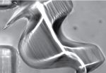
Bioengineers from the UCLA Henry Samueli School of Engineering and Applied Science have developed a new method of 3-D printing that allows production of complex micro-scale objects smaller than the width of a human hair. The technique, using patterned ultraviolet light and a custom-shaped flow of polymer material, creates 3-D objects that can be first designed with software and could be used in a variety of biomedical and industrial applications.
The research was published online in the journal Advanced Materials.
The authors suggest that producing 3-D shapes at the micro scale could be useful for designing custom biomaterials such as interlocking particles that self-assemble to help tissue regenerate, or for industrial applications such as creating new coatings and paints with unique light-reactive properties.
“We know that shape often determines material function, so while we have a few ideas of what this could lead to, this fundamental capability to produce made-to-order 3-D microparticles could be applied in ways we have not contemplated,” said Dino Di Carlo, the principal investigator on the research and a professor of bioengineering at UCLA. “There are so many potential applications — in that sense, it’s really exciting.”
In 3-D printing, a digital blueprint is used to fabricate a wide range of products. The most common method, known as additive fabrication, uses a liquid precursor material that squeezed out of a nozzle, drop by drop. As the liquid hardens, new layers are added until the object is finished. While this and other 3-D printing methods can make shapes with incredible complexity, researchers have not been able to make similarly complex objects smaller than a millimeter because the drops of material are too big.
To make smaller custom objects with folds, holes and other precise features, the UCLA team developed a new technique called optical transient liquid modeling. It uses a series of microfluidic and optical technologies, including a technique previously developed by Di Carlo’s research group that simplifies designing the shape of fluid flows.
First, two different types of fluids are combined in a series of tiny pillars that control the shape of the merged fluids. One fluid is a liquid polymer that is the precursor material for the object. The other essentially acts as a liquid mold for the polymer stream. The arrangement of the pillars determines how the two flows mix and intertwine. The researchers used software that they previously developed to rapidly predict what shape will be produced by altering the pillars’ location and sequence. It can be downloaded for free here.
When the flow of materials is stopped rapidly, an outlined pattern of ultraviolet light — somewhat like a cookie cutter — slices into the precursor stream. So the object is shaped first by the stream, then again by UV light. The UCLA researchers have reached printing speeds of nearly one object every five seconds.
“It’s like we squeeze dough through a mold, which is the liquid mold, to make a noodle and then cut the noodle into pieces using another mold — the patterned UV light,” said Chueh-Yu “Jerry” Wu, the lead author of the research and a graduate student in in Di Carlo’s biomicrofluidics lab.
The objects the team has produced are about 100–500 micrometers in size, with features as small as 10–15 micrometers. With this method, they have produced objects composed of organic materials as well as particles whose movements and position could be precisely controlled by magnetism.
Keegan Owsley, another graduate student in Di Carlo’s lab, is also a co-author of the research.
The research was partially supported by the National Science Foundation. Di Carlo is also a member of the California NanoSystems Institute.
Share on:


Suggested Items
Happy’s Tech Talk #38: Novel Metallization for UHDI
05/07/2025 | Happy Holden -- Column: Happy’s Tech TalkI have been involved in high-density electronics substrates since 1970 when I joined Hewlett-Packard’s RF semiconductor group after college. Figure 1 shows the difference between trace/space lithography for substrates and silicon starting in 1970. My projects involved sapphire circuits for RF devices, but the figure displays the state of PCBs and integrated CMOS circuits and their packaging, not discreet RF devices. Even then, semiconductors were 50X higher density.
Real Time with... IPC APEX EXPO 2025: Emerging Trends in Design and Technology
04/16/2025 | Real Time with...IPC APEX EXPOAndy Shaughnessy speaks with IPC design instructor Kris Moyer to discuss emerging design trends. They cover UHDI technology, 3D printing, and optical data transmission, emphasizing the importance of a skilled workforce. The role of AI in design is highlighted, along with the need for understanding physics and mechanics as designs become more complex. The conversation concludes with a focus on enhancing math skills for better signal integrity.
Real Time with... IPC APEX EXPO 2025: Transition Automation Focusing on Security Coatings and Squeegee Technology
04/16/2025 | Real Time with...IPC APEX EXPOMark Curtin, President of Transition Automation, gives an update on recent innovations at his company. He highlights a record sales month and their new focus on security coatings to fight counterfeiting. Mark explains the engineering behind their durable squeegees, the importance of maintenance, and the value of considering overall costs over just price.
Elephantech: For a Greener Tomorrow
04/16/2025 | Marcy LaRont, PCB007 MagazineNobuhiko Okamoto is the global sales and marketing manager for Elephantech Inc., a Japanese startup with a vision to make electronics more sustainable. The company is developing a metal inkjet technology that can print directly on the substrate and then give it a copper thickness by plating. In this interview, he discusses this novel technology's environmental advantages, as well as its potential benefits for the PCB manufacturing and semiconductor packaging segments.
Flexible Thinking: Flexible Circuit Technology—Looking Back and Forward
03/03/2025 | Joe Fjelstad -- Column: Flexible ThinkingFlexible circuit technology came on the scene as a solution largely for niche applications, however, the technology has emerged in recent years as a cornerstone of modern electronics. Today, the technology is enabling a broad range of new product designs across industries. From wearable devices and medical implants to foldable smartphones and numerous automotive applications, flexible circuits are arguably at the heart of much of the next generation of innovations.