


 Driving Innovation: Mechanical and Optical Processes During Rigid-flex Production
 It’s Only Common Sense: Your Biggest Competitor Is Complacency
 The Chemical Connection: Onshoring PCB Production—Daunting but Certainly Possible


Graphene Proves a Perfect Fit for Wearable Devices
December 30, 2015 | University of ManchesterEstimated reading time: 2 minutes
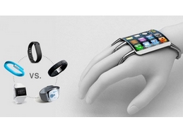
Cheap, flexible, wireless graphene communication devices such as mobile phones and healthcare monitors can be directly printed into clothing and even skin, University of Manchester academics have demonstrated.
In a breakthrough paper in Scientific Reports, the researchers show how graphene could be crucial to wearable electronic applications because it is highly-conductive and ultra-flexible.
The research could pave the way for smart, battery-free healthcare and fitness monitoring, phones, internet-ready devices and chargers to be incorporated into clothing and ‘smart skin’ applications – printed graphene sensors integrated with other 2D materials stuck onto a patient’s skin to monitor temperature, strain and moisture levels.
Examples of communication devices include:
- In a hospital, a patient wears a printed graphene RFID tag on his or her arm. The tag, integrated with other 2D materials, can sense the patient’s body temperature and heartbeat and sends them back to the reader. The medical staff can monitor the patient’s conditions wirelessly, greatly simplifying the patient’s care.
- In a care home, battery-free printed graphene sensors can be printed on elderly peoples' clothes. These sensors could detect and collect elderly people’s health conditions and send them back to the monitoring access points when they are interrogated, enabling remote healthcare and improving quality of life.
Existing materials used in wearable devices are either too expensive, such as silver nanoparticles, or not adequately conductive to have an effect, such as conductive polymers.
Graphene, the world’s thinnest, strongest and most conductive material, is perfect for the wearables market because of its broad range of superlative qualities. Graphene conductive ink can be cheaply mass produced and printed onto various materials, including clothing and paper.
The researchers, led by Dr Zhirun Hu, printed graphene to construct transmission lines and antennas and experimented with these in communication devices, such as mobile and Wifi connectivity.
Using a mannequin, they attached graphene-enabled antennas on each arm. The devices were able to ‘talk’ to each other, effectively creating an on-body communications system.
Page 1 of 2
Share on:


Testimonial
"We’re proud to call I-Connect007 a trusted partner. Their innovative approach and industry insight made our podcast collaboration a success by connecting us with the right audience and delivering real results."
Julia McCaffrey - NCAB GroupSuggested Items
Driving Innovation: Mechanical and Optical Processes During Rigid-flex Production
10/28/2025 | Kurt Palmer -- Column: Driving InnovationRigid-flex printed circuit boards are a highly effective solution for placing complex circuitry in tight, three-dimensional spaces. They are now indispensable across a range of industries, from medical devices and aerospace to advanced consumer electronics, helping designers make the most efficient use of available space. However, their unique construction—combining rigid and flexible materials—presents a fundamental challenge for PCB manufacturers.
SMTAI 2025 Review: Reflecting on a Pragmatic and Forward-looking Industry
10/27/2025 | Marcy LaRont, I-Connect007Leaving the show floor on the final afternoon of SMTA International last week in Rosemont, Illinois, it was clear that the show remains a grounded, technically driven event that delivers a solid program, good networking, and an easy space to commune with industry colleagues and meet with customers.
ITW EAE Despatch Ovens Now Support ASTM 5423 Testing
10/15/2025 | ITW EAEAs the demand for high-performance electrical insulation materials continues to grow—driven by the rapid expansion of electric vehicles (EVs) and energy storage systems—thermal processing has become a critical step in material development.
Beyond Thermal Conductivity: Exploring Polymer-based TIM Strategies for High-power-density Electronics
10/13/2025 | Padmanabha Shakthivelu and Nico Bruijnis, MacDermid Alpha Electronics SolutionsAs power density and thermal loads continue to increase, effective thermal management becomes increasingly important. Rapid and efficient heat transfer from power semiconductor chip packages is essential for achieving optimal performance and ensuring long-term reliability of temperature-sensitive components. This is particularly crucial in power systems that support advanced applications such as green energy generation, electric vehicles, aerospace, and defense, along with high-speed computing for data centers and artificial intelligence (AI).
Is Glass Finally Coming of Age?
10/13/2025 | Nolan Johnson, I-Connect007Substrates, by definition, form the base of all electronic devices. Whether discussing silicon wafers for semiconductors, glass-and-epoxy materials in printed circuits, or the base of choice for interposers, all these materials function as substrates. While other substrates have come and gone, silicon and FR-4 have remained the de facto standards for the industry.