


 Dan’s Biz Bookshelf: ‘The Next RenAIssance: AI and the Expansion of Human Potential’
 The Chemical Connection: When the Industry Moves Faster Than the Standards
 Driving Innovation: Selecting the Right Laser Source


Ventec to Unveil New 'tec-speed' Brand for High Speed/Low Loss Materials at DesignCon 2016
January 13, 2016 | Ventec International GroupEstimated reading time: 2 minutes
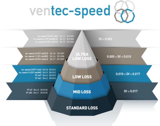
Ventec International Group, a world leader in the production of polyimide & high reliability epoxy laminates and prepregs, will exhibit in Booth 118 at DesignCon 2016 (January 20th to 21st 2016, Santa Clara, CA, USA) where the company will launch a new brand identity, tec-speed, for its high speed/low loss product line. With the launch, Ventec will unveil a new logo, marketing collateral and technical specifications.
The creation of the brand name 'tec-speed' is a move to unite Ventec's high speed/low loss product portfolio and better position the range under a single identity, connecting the products through a clear and cohesive visual presentation.
Martin Cotton, Director OEM Technology, commented: “The tec-speed brand now unites one of the most comprehensive range of products in high speed/low loss PCB material technology. Every tec-speed product provides technological innovation, high performance and quality to customers to perfectly meet their needs.”
Ventec International Group’s COO USA & EUROPE, Mark Goodwin added: “With the growing demand for high reliability and high speed computing & storage applications, and a pipeline of new innovative additions to our range, the timing is right to give our product line a clear identity. More than that, our unique approach to supply chain ownership, with a manufacturing and distribution network that covers the relevant markets globally, ensures fast delivery of quality materials”.
A selection of products will be highlighted at the show, including:
tec-speed 6.1 (Dk 3.2, Df 0.004 RC 50%) - Ultra-Low Loss High Tg material available with all copper styles, including HVLP. Uses Low Dk spread glass to improve Skew and Jitter. Applications include Telecom, Router, Servers etc. Specifically, backplane and daughter card designs where good Signal Integrity is essential. This material has excellent Thermal properties.
tec-speed 4.0 (Dk 3.8, Df 0.007) - Low-Loss High Tg material available with all copper styles, including HVLP. Applications focus on High Frequency & High Speed designs, Automotive and Satellite communication, Navigation, GPS, etc. are typical applications. This material has excellent thermal properties.
tec-speed 1.0 (Dk 3.9, Df 0.012 @ 10GHz RC75%) - Mid-Loss Mid Tg Halogen Free material available with all copper styles. Applications include hand-held products, specifically those that require high frequency high speed materials. This material has excellent thermal properties.
For more information about Ventec’s solutions and the company’s wide variety of products, please visit www.venteclaminates.com or download to the Ventec APP.
About Ventec International
With volume manufacturing facilities and HQ in Suzhou China, Ventec International specializes in advanced copper clad glass reinforced and metal backed substrates for the PCB industry. With distribution locations and quick-turn CCL manufacturing sites in both the US and Europe, Ventec International is a premier supplier to the Global PCB industry. For more information, visit www.venteclaminates.com, www.ventec-usa.com or www.ventec-europe.com.
Share on:


Testimonial
"In a year when every marketing dollar mattered, I chose to keep I-Connect007 in our 2025 plan. Their commitment to high-quality, insightful content aligns with Koh Young’s values and helps readers navigate a changing industry. "
Brent Fischthal - Koh YoungSuggested Items
Driving Innovation: Selecting the Right Laser Source
04/28/2026 | Simon Khesin -- Column: Driving InnovationWhen I first joined Schmoll Maschinen, I brought experience from almost every PCB process, except for laser. As I immersed myself in laser processing, I realized why it can seem so daunting to a newcomer. The complexity arises from three intersecting factors: A vast variety of laser sources: CO2, UV-nano, green-pico, UV-pico, IR-pico, and others; a diverse range of applications: Drilling, cutting, ablation, and more; and an extensive list of materials: These have vastly different absorption rates. Choosing the right machine or laser source is rarely trivial. Even for experienced engineers, answering "Which source is best?" requires examining the business's specific goals.
Institute of Circuit Technology Spring Seminar 2026: A Bright Future in Europe
04/23/2026 | Pete Starkey, I-Connect007Through the leafy lanes and spring flowers of Warwickshire and back to Meridan, the traditional centre of England, and now officially part of the Metropolitan Borough of Solihull in the county of the West Midlands, I attended the Annual General Meeting and Spring Seminar of the Institute of Circuit Technology (ICT) on April 14. Out of the AGM came notable changes in leadership at the top of the Institute: the retirement of Mat Beadel as chair and Emma Hudson as technical director. Effective May 1, Steve Driver is the new chair, and Alun Morgan is the new technical director.
ACCM Unveils Negative and Near-zero CTE Materials for Large-Format AI Chips
04/21/2026 | Advanced Chip and Circuit MaterialsAdvanced Chip and Circuit Materials, Inc. (ACCM) has launched two new materials: Celeritas HM50, with a negative coefficient of thermal expansion (CTE) of -8 ppm/°C to offset the positive CTE and expansion of copper with temperature on circuit boards, and Celeritas HM001, with near-zero CTE and the low-loss performance needed for high-speed signal layers to 224 Gb/s and faster in artificial intelligence (AI) circuits.
Fresh PCB Concepts: Designing PCBs for Harsh Environments—Reliability Is Engineered Upstream
04/23/2026 | Team NCAB -- Column: Fresh PCB ConceptsWhen engineers hear the phrase “harsh environment,” they usually think of the extreme temperature swings, vibration and shock, pressure changes, or radiation in aerospace. However, aerospace is not the only harsh environment where electronic assemblies must survive. Automotive power electronics, downhole oil and gas tools, marine controls, rail systems, defense platforms, and industrial automation equipment all expose PCBs to environments that are equally unforgiving. The stress mechanisms may differ, but the physics does not.
Advanced Packaging for AI: Reliability Starts at the Cu/Cu/Cu Microvia Junction
04/20/2026 | Kuldip Johal, MKS' AtotechThe rapid growth of AI computing, from training clusters to inference at scale, is reshaping demand across the entire electronics supply chain. Advances in technology requirements, such as higher bandwidth, lower latency, and greater compute density, are driving the development of advanced packaging technologies and transforming the PCB industry across design, manufacturing, testing, and even architecture.