


 Beyond the Board: How a Diminished Supplier Base Affects Complex PCB Manufacturing Readiness in Defense
 Defense Speak Interpreted: Hypersonics Report Back After Six Years of Silence
 American Made Advocacy: American Microelectronics Power the Future of High Technology


Configurable Analog Chip Computes with 1,000 Times Less Power than Digital
March 3, 2016 | Georgia TechEstimated reading time: 5 minutes
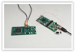
Researchers have built and demonstrated a novel configurable computing device that uses a thousand times less electrical power – and can be built up to a hundred times smaller – than comparable digital floating-gate configurable devices currently in use.
The new device, called the Field-Programmable Analog Array (FPAA) System-On-Chip (SoC), uses analog technology supported by digital components to achieve unprecedented power and size reductions. The researchers said that for many applications these low-power analog-based chips are likely to work as well as or better than configurable digital arrays.
Currently, field programmable gate arrays (FPGAs) – digital devices widely used in consumer devices, defense systems and more – dominate the configurable chip market. These floating-gate integrated circuits can be altered internally at any time, and techniques to reconfigure them for many different forms and functions are well established.
Professionals familiar with FPGAs will find the programming interface of the new analog chip surprisingly like the digital circuits in many ways, said Jennifer Hasler, a professor in the Georgia Tech School of Electrical and Computer Engineering (ECE) and leader of the research team that produced the new analog architecture.
“But in other ways the FPAA is going to seem quite different,” she said. “In terms of the power needed, it's extremely different because you need only milliwatts to run the analog device, while it’s hard to get an FPGA to work on less than a watt.”
A paper on the new FPAA system-on-chip device has been published on the IEEE Xplore website. Another paper focusing on the details of programming FPAA devices was also published on the Xplore site. In addition a third paper, detailing a high-level open-source programming toolset developed by Hasler and her team for programming analog arrays, has also been published online in the Journal of Low Power Electronics and Applications.
Novel Techniques
Traditionally, analog technology has been used primarily for hard-wired circuits such as sensors that interface between digital devices and the real world; examples include the circuits that detect and reproduce sound in cell phones and other devices. Analog circuits are also used extensively in electronics to regulate and optimize power use. These single-function circuits cannot perform software-based computation, using hardware gates and switches, in the manner of digital integrated circuits.
Hasler’s team, however, has developed techniques that perform computation using an analog-style physical architecture by reliably positioning electrons in an FPAA’s connective structure. This approach stands in contrast to FPGAs, which process electrons through floating gates in ways similar to conventional digital semiconductors such as memory chips or central processing units.
One advantage of FPAAs is that they're non-volatile, Hasler explained, meaning they retain data even when power is turned off. This is similar to flash memory technology, such as the solid-state drives and storage cards commonplace today. The use of non-volatile memory reduces power consumption, in contrast to the higher power needs of the volatile SRAM configurations typically used in FPGAs.
“In addition to being non-volatile, our analog architecture lets us do something fairly radical – we can compute using the routing fabric of the chip, exploiting areas that are usually considered just dead weight,” Hasler said. “To help do this, we've developed highly efficient switches that can be programmed on, off, or in-between – partially on and partially off. This flexibility provides both increased computation capabilities and reduced power consumption.”
Milliwatts or Microwatts
The present FPAA device can operate on less than 30 milliwatts – thousandths of a watt, Hasler explained. That level approaches three orders of magnitude less than a conventional digital configurable chip. Further design advances in analog arrays could bring their power needs down into the microwatt range – millionths of a watt.
To program the analog environment of the new device, researchers manipulate electrons in precise ways. Using electron-injection and electron-tunneling techniques, they erase data by lowering the number of electrons at specific locations in the device structure to the lowest possible value. Then they encode new data by increasing the number of electrons located at a given location up to an exact value.
This complex approach makes possible a highly dense chip structure that offers many parameters – meaning programmable variables that can exist in a large number of different states and offer many shadings of behavior. It is this structural density that allows greater computing capability for a given degree of physical size and power input.
“Our FPAA chip has roughly half a million of these programmable parameters,” Hasler said. “They can be used as a switch in a digital manner – using the lowest possible value for ‘off’ or the highest possible value for ‘on’ – or we can achieve even more rich behavior using intermediate values.”
Page 1 of 2
Share on:


Testimonial
"Advertising in PCB007 Magazine has been a great way to showcase our bare board testers to the right audience. The I-Connect007 team makes the process smooth and professional. We’re proud to be featured in such a trusted publication."
Klaus Koziol - atgSuggested Items
EMI Promotes David Vue to Lead Military and Aerospace Division
03/31/2026 | Express Manufacturing Inc.Express Manufacturing, Inc. (EMI), a global electronics manufacturing services (EMS) provider, announced the promotion of David Vue to Military and Aerospace Division Manager.
Mobix Labs Secures Significant U.S. Navy Tomahawk Missile Component Order as Production Accelerates
03/04/2026 | BUSINESS WIREMobix Labs, Inc., a provider of 5G mmWave, defense, and aerospace components, today announced receipt of a significant production purchase order for components used in the U.S. Navy’s Tomahawk cruise missile program.
Lockheed Martin Demonstrates Next-Gen Command and Control at Lightning Surge 1
01/26/2026 | Lockheed MartinIn collaboration with the 25th Infantry Division (25ID), CPE C3N, multiple U.S. Army stakeholders and several industry partners including Raft and Accelint, Lockheed Martin delivered and successfully demonstrated the first iteration of a Next Generation Command and Control (NGC2) prototype at Lightning Surge 1 (LS1).
Mil Aero High Speed Connectors Market Report 2026: $7.41 Bn Opportunities, Trends, Competitive Landscape, Strategies, and Forecasts, 2020-2025, 2025-2030F, 2035F
01/20/2026 | GlobeNewswireThe Mil Aero High-Speed Connectors Market Global Report 2026 offers strategists, marketers, and senior management the essential data to evaluate this swiftly developing market. The report predicts and analyzes trends that will influence the sector in the next decade and beyond, providing a roadmap to capture emerging opportunities.
Teledyne FLIR Wins $32M Recon Surveillance Contract in Bulgaria
01/15/2026 | BUSINESS WIRETeledyne FLIR Defense, part of Teledyne Technologies Incorporated, announced that it has been awarded a contract by the U.S. Army worth up to $32 million to deliver and integrate advanced electro-optical (EO/IR) systems for the Stryker Infantry Carrier Vehicle (ICV) Recon Kit.