-

- News
- Books
Featured Books
- design007 Magazine
Latest Issues
Current Issue
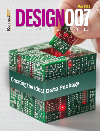
Creating the Ideal Data Package
Why is it so difficult to create the ideal data package? Many of these simple errors can be alleviated by paying attention to detail—and knowing what issues to look out for. So, this month, our experts weigh in on the best practices for creating the ideal design data package for your design.

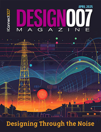
Designing Through the Noise
Our experts discuss the constantly evolving world of RF design, including the many tradeoffs, material considerations, and design tips and techniques that designers and design engineers need to know to succeed in this high-frequency realm.

Learning to Speak ‘Fab’
Our expert contributors clear up many of the miscommunication problems between PCB designers and their fab and assembly stakeholders. As you will see, a little extra planning early in the design cycle can go a long way toward maintaining open lines of communication with the fab and assembly folks.
- Articles
- Columns
Search Console
- Links
- Media kit
||| MENU - design007 Magazine
Designers and Design Engineers: Two Sides of the Same Coin
June 1, 2016 | Andy Shaughnessy, PCBDesign007Estimated reading time: 2 minutes
Andy and Sue Critcher have been the lead designers at Total Board Solutions Limited, a UK-based design bureau, since its founding in 1998. I asked Andy to share his opinion about the friction between some PCB designers and their engineers, and what can be done to improve communications between these groups.
Andy Shaughnessy: Andy, tell us a little bit about your company and how you operate.
Andy Critcher: Total Board Solutions Limited (TBS) is a design services bureau based in the UK. We fit into our customer’s design process, providing whatever is not a core competency. This means that for some customers we perform just the layout portion of their design while for others we enter the schematic, libraries, create the layout and even get the boards fabricated and assembled—no two customers are exactly the same. When working with startups we provide the link between the concept, or idea, and product realization; providing knowledge of design process, fabricators capabilities and our experience when discussing the inevitable tradeoffs between the requirement and what is possible.
Shaughnessy: A recent survey of our PCB designer readers found that there’s often friction between PCB designers and engineers. Some designers say, only half-jokingly, that their EEs are their biggest challenge. Why do you think there’s such disconnect?
Critcher: Looking solely from the PCB side, I think that the disconnect mainly arises from the lack of understanding of what a PCB designer actually does, it is perceived as a simple task of dot joining and that anyone can do it. I know that this is a bit of a cliché but it does seem to hold true. As an example, in a number of the companies that I have worked with, PCB progress meetings are held and the PCB designer is never asked to attend; their input can be easily be determined by the engineering team/project manager.
This perception is backed up by the lack of formal qualification for PCB designers—for my generation, we generally started off as mechanical draughtsman in the traditional drawing office and then moved to the PCB section.
This perception means that the status of the PCB designer is quite low, so when they advise the engineer that something is not possible this can be met with a certain amount of derision. The engineer possibly thinks that the PCB designer is just being obstructive, while conversely, the PCB designer thinks that the engineer is very dismissive of his knowledge, capabilities, opinion, etc.
Let’s look at the issue from the engineer’s perspective. By providing design consultancy, we are fortunate enough to be a lot more involved in the engineer’s world, including some of the problems that they have to deal with as part of the overall product development. One engineer explained that the design part was relatively straightforward, but the need to meet cost, functionality, component sourcing, obsolescence, test plans, as well as reading through 150+ pages of documentation on a device’s timing “makes life interesting.” As PCB designers, we tend to have a lot of questions, especially about the newer technology, so we can bombard the engineer with a number of questions concerning unfamiliar topics expecting immediate answers, and normally at this point the pressure to get it finished is already building.
To read this entire article, which appeared in the April 2016 issue of The PCB Design Magazine, click here.
Suggested Items
RF PCB Design Tips and Tricks
05/08/2025 | Cherie Litson, EPTAC MIT CID/CID+There are many great books, videos, and information online about designing PCBs for RF circuits. A few of my favorite RF sources are Hans Rosenberg, Stephen Chavez, and Rick Hartley, but there are many more. These PCB design engineers have a very good perspective on what it takes to take an RF design from schematic concept to PCB layout.
Cadence Unveils Millennium M2000 Supercomputer with NVIDIA Blackwell Systems
05/08/2025 | Cadence Design SystemsAt its annual flagship user event, CadenceLIVE Silicon Valley 2025, Cadence announced a major expansion of its Cadence® Millennium™ Enterprise Platform with the introduction of the new Millennium M2000 Supercomputer featuring NVIDIA Blackwell systems, which delivers AI-accelerated simulation at unprecedented speed and scale across engineering and drug design workloads.
The Right Blend: Mixed Wireless Technologies
05/08/2025 | Kirsten Zima, Siemens EDAA common trend recently is to employ as many radios as possible on a single PCB. With the increase of wireless standards and the downscaling of PCB size, it can be difficult to know what the most critical design parameters are to focus on. In this article, we’ll discuss the most important considerations to make when designing with mixed wireless technologies, such as Bluetooth, GPS, and Wi-Fi, on a single PCB. These considerations include antennas, frequencies, FCC compliance, shielding, and layout with and without transition vias.
ZESTRON Announces New Reliability and Solutions Service for Risk Assessment & Mitigation of Electronic Assemblies
05/06/2025 | ZESTRONZESTRON, the leading global provider of high-precision cleaning products, services, and training solutions, is thrilled to introduce its new Reliability and Solutions (R&S) service.
PCB East Continues to Expand
05/06/2025 | Andy Shaughnessy, Design007 MagazineIt was a perfect week for a conference and trade show in metropolitan Boston, with high temperatures in the 70s. PCB East took place at the Boxboro Regency Hotel and Conference Center April 29–May 2, with the expo on April 30. PCB East has been expanding since its relaunch a few years ago, with conference and show attendance rising each year.


