












 It’s Only Common Sense: How AI Consumes the Electronics Supply Chain
 Dan’s Biz Bookshelf: ‘Building a Story Brand 2.0’





If you want to save on your monthly electric bill and reduce your greenhouse gas emissions at the same time, you might buy a new, energy-efficient refrigerator. Or water heater. Or clothes dryer. But if you can only replace one of these, which will give you the biggest payback?
You could try to figure that out by comparing the energy-use labels from your existing appliances with those of the models you might purchase — if you still have your old labels. Even then, the numbers may differ significantly from your actual usage, depending on factors such as age, condition, and your local climate. But soon, there could be a much easier way to figure out exactly how much power is being used by every appliance, lighting fixture, and device in your home, with pinpoint accuracy and at low cost, thanks to devices and software developed by researchers at MIT.
The team’s findings, developed over several years of intensive research, are described in a series of papers, including one published this week in the IEEE Sensors Journal, in a paper by MIT Professor of Electrical Engineering Steven Leeb and recent graduates David Lawrence MEng ’16 and John Donnal PhD ’16. Another paper from the team, which also includes as co-author James Paris PhD ’13, is still in press.
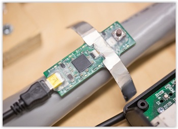
While many groups have worked on developing devices to monitor electricity use, the new MIT system has some key advantages over other approaches. First, it involves no complex installation: No wires need to be disconnected, and the placement of the postage-stamp-sized sensors over the incoming power line does not require any particular precision — the system is designed to be self-calibrating. Second, because it samples data very quickly, the sensors can pick up enough detailed information about spikes and patterns in the voltage and current that the system can, thanks to dedicated software, tell the difference between every different kind of light, motor, and other device in the home and show exactly which ones go on and off, at what times.
Own your own data
Perhaps most significantly, the system is designed so that all of the detailed information stays right inside the user’s own home, eliminating concerns about privacy that potential users may have when considering power-monitoring systems. The detailed analysis, including the potential for specialized analysis based on an individual user’s specific needs or interests, can be provided by customized apps that can be developed using the MIT team’s system.
Tests of the system have showed its potential to save energy and greenhouse emissions — and even to improve safety. One installation at a military base used for training exercises revealed that large tents were being heated all day during winter months, even though they were unoccupied for most of the daytime hours — a significant waste of money and fuel (which, in a combat setting, could be an important logistical concern). Another test installation, in a home, found an anomalous voltage pattern that revealed a wiring flaw that caused some copper plumbing pipes to carry a potentially dangerous live voltage.
“For a long time, the premise has been that if we could get access to better information [about energy use], we would be able to create some significant savings,” Leeb says. He and his students have been tackling the problem for more than 10 years and bit by bit have found ways to circumvent the daunting problems involved in achieving this basic task.
First was the ability to monitor changes in voltage and current without cutting the main incoming power line to a home or business (an expensive process requiring a licensed electrician) or plugging every appliance into a special monitoring device. Other groups have attempted to use wireless sensors to pick up the very faint magnetic and electric fields near a wire, but such systems have required a complex alignment process since the fields in some places can cancel each other out. The MIT team solved the problem by using an array of five sensors, each slightly offset from the others, and a calibration system that tracks the readings from each sensor and figures out which one is positioned to give the strongest signal.
Page 1 of 2
Share on:



Subscribe
Stay ahead of the technologies shaping the future of electronics with our latest newsletter, Advanced Electronics Packaging Digest. Get expert insights on advanced packaging, materials, and system-level innovation, delivered straight to your inbox.
Subscribe now to stay informed, competitive, and connected.
Suggested Items
Flex Connections: Material Selection in Nickel vs. Copper Tabs
09/17/2026 | Zack Schaner -- Column: Flex ConnectionsFlexible printed circuits are being designed to do more than route signals. In many applications, the flex circuit must also provide robust electrical interfaces, mechanical reinforcement, and reliable transitions between the circuit and surrounding assemblies. One effective way to accomplish this is by integrating copper or nickel tabs directly into a flexible printed circuit.
Secure PCB Sourcing Is Not Enough
09/15/2026 | Ryan O'Connor, SOMACISDefense teams are paying much closer attention to where their PCB work goes. That’s a smart approach. Approved suppliers, secure data, domestic production, and proper certifications all matter. But these factors do not address the tougher question: Does this specific board actually fit the supplier’s process? This is where sourcing decisions often become too general. A supplier might be approved and certified, but that does not mean every complex defense board is right for their shop.
Evaluating Physical Process Parameters to Improve Copper Plating Distribution
09/11/2026 | Richard Nichols and Marko Mirkovic, GreenSource EngineeringConsistent copper thickness across panels directly affects etching accuracy, conductor geometry, electrical performance, and ultimately, product reliability. It is a persistent manufacturing challenge, and for PCB fabricators serving advanced markets—including RF applications, power electronics, and other high-performance technologies—electrolytic copper plating is one of the most critical process steps. In response, manufacturers typically modify shielding, rectification, or tooling, which may require an expensive hardware change.
MKS Highlights Laser and Chemistry Solutions at KPCA Show 2026
09/03/2026 | AtotechMKS Inc. will showcase integrated manufacturing solutions in advanced packaging, package substrate, and printed circuit board (PCB) manufacturing at KPCA Show 2026 held at Songdo Convensia in Incheon, South Korea, from September 9–11. Visitors can meet MKS’ representatives at booth 201 in hall 3 and discover the company’s latest solutions for advanced electronics manufacturing.
Trouble in Your Tank: Pre-electroless Causes of Voids
09/02/2026 | Michael Carano -- Column: Trouble in Your TankTo support advanced 2.5D and 3D heterogeneous integration, product and motherboard designs are now using higher layer counts. As layer counts increase, plated through-holes (PTHs) become deeper and higher in aspect ratio, making it more difficult to achieve a continuous, void-free copper deposit. Drilling these thicker panels and higher aspect ratio vias adds another layer of complexity. Since there are many potential causes of PTH voiding, I’ll focus on pre-electroless copper causes, including drilling.