


 Trouble in Your Tank: Implementing Direct Metallization in Advanced Substrate Packaging
 It’s Only Common Sense: Storytelling That Sells—Stop Pitching, Start Painting Pictures
 The Right Approach: Get Ready for ISO 9001 Version 6


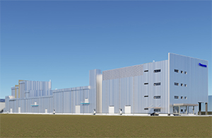
AT&S Tech Days in Santa Clara - Update of the Latest Trends in PCB Technologies
September 1, 2016 | AT&SEstimated reading time: 1 minute
AT&S Americas, LLC is organizing the AT&S Tech Days on September 12-13 in Santa Clara, California. During the first day technical seminars and presentations from AT&S and partners will highlight the latest innovations and market trends for PCB technology. The event will take place at the Santa Clara convention centre. On the second day AT&S offers individualized company forums with its experts at the Santa Clara Hyatt Regency Hotel.
Hosted by Scott Clifford, President AT&S Americas LLC, the presentations will start with an overview of the technology drivers impacting the next generation ofPCB technology. Hannes Voraberger, Group Manager AT&S R&D will describe how PCB and substrate technologies will merge providing continued miniaturization. This technology oriented presentation will be followed by an industry outlook analyzing the key market trends driving interconnect technology, given by Prismark Partners, an electronics industry consulting firm. A customer perspectiveexplaining the 3D system supply chain integration will be presented by the UTAC Group.
Other speakers will address the design for embedded technology with focus on thinner formats and higher integration as well as mobile design considerations like performance, density, cycle time and material.
In addition, PCB flex & rigid technologies and applications, power electronics and thermal management options, mechanical integration and 3D technologies, high-speed and high-frequency in PCB manufacturing are being addressed by the experts.
The complete agenda is available HERE.
Visitors can register HERE.
About AT&S
AT&S is the European market leader and one of the globally leading manufacturers of high-value printed circuit boards. AT&S industrialises leading-edge technologies for its core business segments Mobile Devices, Automotive, Industrial, Medical and Advanced Packaging. In 2016, AT&S will produce two new, leading-edge technologies at the new site in Chongqing (China) – IC substrates and substrate-like printed circuit boards for high-end applications. As an international growth enterprise, AT&S has a global presence, with production facilities in Austria (Leoben and Fehring) and plants in India (Nanjangud), China (Shanghai, Chongqing) and Korea (Ansan, near Seoul). The company employed an average of 8,688 people as of December 31, 2015.
Share on:


Testimonial
"In a year when every marketing dollar mattered, I chose to keep I-Connect007 in our 2025 plan. Their commitment to high-quality, insightful content aligns with Koh Young’s values and helps readers navigate a changing industry. "
Brent Fischthal - Koh YoungSuggested Items
AI-Powered Wearables Transform How Consumers Interact with Everyday Technology
09/15/2025 | PR NewswireThe global demand for AI-driven, touchless wearable technologies is accelerating as consumers seek more natural, seamless and intuitive ways to interact with their devices. Traditional touch screens and voice assistants, while effective, are increasingly viewed as limiting in a world where multitasking, mobility and efficiency are key. As industries from consumer electronics to augmented reality and enterprise computing embrace the possibilities of gesture-based control, the market for neural interfaces is rapidly expanding
Hanwha Aerospace to Collaborate with BAE Systems on Advanced Anti-jamming GPS for Guided Missiles
09/15/2025 | HanwhaHanwha Aerospace has signed a contract with BAE Systems to integrate next-generation, anti-jamming Global Positioning System (GPS) technology into Hanwha Aerospace’s Deep Strike Capability precision-guided weapon system.
United Electronics Corporation Unveils Revolutionary CIMS Galaxy 30 Automated Optical Inspection System
09/11/2025 | United Electronics CorporationUnited Electronics Corporation (UEC) today announced the launch of its new groundbreaking CIMS Galaxy 30 Automated Optical Inspection (AOI) machine, setting a new industry standard for precision electronics manufacturing quality control. The Galaxy 30, developed and manufactured by CIMS, represents a significant leap forward in inspection technology, delivering exceptional speed improvements and introducing cutting-edge artificial intelligence capabilities.
Intel Announces Key Leadership Appointments to Accelerate Innovation and Strengthen Execution
09/09/2025 | Intel CorporationIntel Corporation today announced a series of senior leadership appointments that support the company’s strategy to strengthen its core product business, build a trusted foundry, and foster a culture of engineering across the business.
DARPA, State of New Mexico Establish Framework to Advance Quantum Computing
09/08/2025 | DARPAAs part of the Quantum Benchmarking Initiative (QBI), DARPA signed an agreement with the State of New Mexico’s Economic Development Department to create the Quantum Frontier Project.