


 Marcy’s Musings: Thank You, Columnists!
 It’s Only Common Sense: Stop Pretending Your Customers Are Loyal
 Happy’s Tech Talk #44: Memories of the ‘Mystery Systems of the East’


Continuous Roll-process Technology for Transferring and Packaging Flexible Large-scale Integrated Circuits
September 2, 2016 | KAISTEstimated reading time: 1 minute
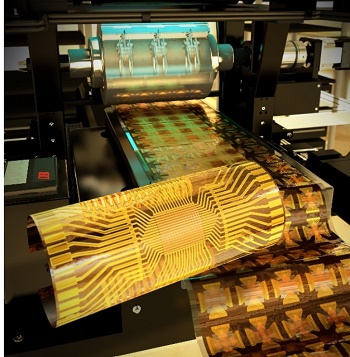
A research team led by Professor Keon Jae Lee from the Korea Advanced Institute of Science and Technology (KAIST) and by Dr. Jae-Hyun Kim from the Korea Institute of Machinery and Materials (KIMM) has jointly developed a continuous roll-processing technology that transfers and packages flexible large-scale integrated circuits (LSI), the key element in constructing the computer’s brain such as CPU, on plastics to realize flexible electronics.
Professor Lee previously demonstrated the silicon-based flexible LSIs using 0.18 CMOS (complementary metal-oxide semiconductor) process in 2013 (ACS Nano, “In Vivo Silicon-based Flexible Radio Frequency Integrated Circuits Monolithically Encapsulated with Biocompatible Liquid Crystal Polymers”) and presented the work in an invited talk of 2015 International Electron Device Meeting (IEDM), the world’s premier semiconductor forum.
Highly productive roll-processing is considered a core technology for accelerating the commercialization of wearable computers using flexible LSI. However, realizing it has been a difficult challenge not only from the roll-based manufacturing perspective but also for creating roll-based packaging for the interconnection of flexible LSI with flexible displays, batteries, and other peripheral devices.
To overcome these challenges, the research team started fabricating NAND flash memories on a silicon wafer using conventional semiconductor processes, and then removed a sacrificial wafer leaving a top hundreds-nanometer-thick circuit layer. Next, they simultaneously transferred and interconnected the ultrathin device on a flexible substrate through the continuous roll-packaging technology using anisotropic conductive film (ACF). The final silicon-based flexible NAND memory successfully demonstrated stable memory operations and interconnections even under severe bending conditions. This roll-based flexible LSI technology can be potentially utilized to produce flexible application processors (AP), high-density memories, and high-speed communication devices for mass manufacture.
Professor Lee said, “Highly productive roll-process was successfully applied to flexible LSIs to continuously transfer and interconnect them onto plastics. For example, we have confirmed the reliable operation of our flexible NAND memory at the circuit level by programming and reading letters in ASCII codes. Out results may open up new opportunities to integrate silicon-based flexible LSIs on plastics with the ACF packing for roll-based manufacturing.”
Dr. Kim added, “We employed the roll-to-plate ACF packaging, which showed outstanding bonding capability for continuous roll-based transfer and excellent flexibility of interconnecting core and peripheral devices. This can be a key process to the new era of flexible computers combining the already developed flexible displays and batteries.”
Share on:


Testimonial
"Our marketing partnership with I-Connect007 is already delivering. Just a day after our press release went live, we received a direct inquiry about our updated products!"
Rachael Temple - AlltematedSuggested Items
Enhancing Reliability in Harsh Environments
11/18/2025 | Real Time with...SMTAISLB is a leading technology OEM in the energy sector, providing technology, equipment, and services to support oil exploration, drilling, production, and processing. This is big business, and the technology can be complex. Chintan Sanghani—a new voice in SMT007 Magazine—is SLB’s expert in quality and process improvement, and I had the opportunity to meet him while in Chicago in October.
Ynvisible Reports Commercial Momentum and Expanding Market Engagements in 2025/2026
11/18/2025 | Ynvisible Interactive Inc.Ynvisible Interactive Inc., a leading provider of ultra-low power printed e-paper display solutions, is pleased to provide an update on its commercial activities and market engagement for 2025.
Voices of the Industry Features Elephantech’s Satoshi Konagai on the Future of Sustainable PCB Manufacturing
11/17/2025 |I-Connect007 is pleased to announce the release of the latest episode in its acclaimed podcast series, Voices of the Industry. In this episode, host Marcy LaRont speaks with Satoshi Konagai, Executive Officer and Head of Marketing of Elephantech, about the company’s groundbreaking additive manufacturing technology that’s reshaping the printed circuit board (PCB) industry.
Setting the Standards for AI-era Packaging: Key Takeaways from IMPACT 2025
11/17/2025 | Sydney Xiao, Global Electronics Association East AsiaDiscussions on component-to-system-level integration took center stage at the International Microsystems, Packaging, Assembly and Circuits Technology (IMPACT) 2025, Asia-Pacific’s leading conference for microsystems, packaging, and circuit technology, which celebrated its 20th year in October. Co-organized and supported by the Global Electronics Association, the event in Taipei, Taiwan, brought global industry leaders together to explore how packaging innovations are shaping the AI era.
I-Connect007 Editor’s Choice: Five Must-Reads for the Week
11/14/2025 | Nolan Johnson, I-Connect007I read an interesting article this week about a breakthrough on building microprocessors to run on microwaves rather than traditional digital circuitry. It cites an academic study that begins, “The development of high-bandwidth applications, including multi-gigabit communication and radar imaging, demands faster processing. However, in the microwave regime, where frequencies exceed clock rates, sampling and computation become challenging. Here we report an integrated microwave neural network for broadband computation and communication.”