


 The Doctor’s In: Reliability in the Delivery Room
 Marcy’s Musings: The ‘Magic’ of Additive Processes
 It’s Only Common Sense: More Great Business Ideas from ‘Breaking Bad’
Study: Raising Temperature Changes an Element's Electronic "Topology"
November 1, 2016 | CaltechEstimated reading time: 2 minutes
Materials scientists at Caltech have discovered a new way that heat tweaks the physical properties of a material.
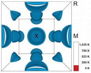
Experimenting with an alloy of iron and titanium (FeTi), a team led by Caltech's Brent Fultz found that increasing heat alters the topology of the material's Fermi surface—an abstract map of the allowable energy states that can be occupied by electrons.
Fultz, the Barbara and Stanley R. Rawn, Jr., Professor of Materials Science and Applied Physics in the Division of Engineering and Applied Science, likens a Fermi surface to a planet covered by a smooth ocean and rocky landmasses. The ocean is made up of electrons, while the land represents voids where electrons are not present. Placing an element under extreme pressure—like that in Earth's core—can cause landforms lurking just below the surface to emerge, in turn altering where electrons are likely to be found. The appearance of these new features in a Fermi surface is called an electronic topological transition (ETT). The concept of an ETT was proposed by the Russian physicist I. M. Lifshitz in 1960, and ETTs have been observed by subjecting metals to pressures on the order of 100,000 atmospheres.
Heating causes electrons to slosh around within the Fermi surface, but, as with waves moving on water, the coastlines—the boundaries between electrons and electron-less voids—remain about the same. However, Fultz and his colleagues noticed that because heat also displaces atoms, heating can in some cases reveal landforms hidden below the surface of that metaphorical Fermi sea.
In practical terms, altering the topology of the Fermi surface alters the chemical properties of a metal or alloy, which in turn alters its electrical conductivity.
The potential value to engineers lies in the fact that it is much easier to raise the temperature of a material than it is to place it under the sort of pressure needed to force an ETT. "The pressures needed to cause an ETT are intense, while the temperature changes needed are comparatively low," says Fultz. Indeed, gigapascals of pressure are required to cause an ETT—that is, tens of thousands of times the pressure of Earth's atmosphere. However, Fultz and his colleagues noted ETTs occurring within hundreds of degrees Fahrenheit of temperature change.
The discovery was something of an accident—the result of computationally chasing down anomalous results while performing neutron scattering tests on an FeTi alloy that is of interest to engineers because it is remarkably strong and stretchable.
Neutron scattering reveals details about a material's atomic structure. In the method, a beam of neutrons is fired at a material and the energies and angles of the scattered neutrons are recorded and analyzed. In particular, Fultz's group was using neutron scattering to study the vibrations of atoms in crystals, which almost always move and buzz slightly. The researchers found that, with increasing temperatures, the specific patterns of buzzing changed dramatically in a way that could not be explained through known mechanisms.
Caltech graduate student Fred Yang (MS '15), lead author of a paper about the discovery appearing in the journal Physical Review Letters, ran numerous computer simulations that suggested the temperature-related change could be explained by an ETT in FeTi.
Next, Fultz and Yang plan to explore other elements with features lurking just below their Fermi surfaces.
Share on:


Suggested Items
SEMICON Europa 2024 Call for Abstracts Opens
05/21/2024 | SEMISEMI Europe announced the opening of the Call for Abstracts for SEMICON Europa 2024, to be held November 12-15 at Messe München in Munich, Germany. Selected speakers will share their expertise at the Advanced Packaging Conference (APC), Fab Management Forum (FMF), MEMS & Imaging Sensors Summit and during presentations on the show floor.
Material Insight: The Dielectric Constant of PCB Materials
05/17/2024 | Dr. Preeya Kuray -- Column: Material InsightIn the world of PCB design, miniaturization can be achieved by using low dielectric constant (Dk) materials. Low Dk materials can allow for a reduction in thickness while maintaining a given trace width, leading to lower transmission loss and higher density circuitry.
IPC APEX EXPO: Some Thoughts About Growth
05/16/2024 | Dan Feinberg, I-Connect007After two and a half days of wandering the aisles at IPC APEX EXPO 2024, for the first time, I almost felt like I was exploring CES. There were so many booths and exhibits that I could describe, but I’d like to focus on the growth and huge value of this event, which has expanded well beyond just the growing and impressive exhibit show floor.
The Shaughnessy Report: Unlock Your High-speed Material Constraints
05/15/2024 | Andy Shaughnessy -- Column: The Shaughnessy ReportThe world of PCB materials used to be a fairly simple one. It was divided into two groups: the “traditional” laminates, often called FR-4, and the high-speed laminates developed especially for high-speed PCBs. These were two worlds that usually didn’t collide. But then traditional laminates started getting better, and high-speed designers and design engineers took notice and started to reconsider what FR-4 could be used for.
Breaking High-speed Material Constraints: Design007 Magazine — May 2024
05/14/2024 | I-Connect007 Editorial TeamDo you need specialty materials for your high-speed designs? Maybe not. Improvements in resins mean designers of high-speed boards can sometimes use traditional laminate systems instead of high-speed materials, saving time and money while streamlining the fab process. In the May 2024 issue of Design007 Magazine, our contributors explain how to avoid overconstraining your materials when working with high-speed boards.