


 Material Insight: The Dielectric Constant of PCB Materials
 American Made Advocacy: What About the Rest of the Technology Stack?
 It’s Only Common Sense: Great Ideas From John Mitchell’s Book on Hiring Habits
Miniscule Amounts of Impurities in Vacuum Greatly Affecting OLED Lifetime
December 29, 2016 | Kyushu UniversityEstimated reading time: 2 minutes
Reproducibility is a necessity for science but has often eluded researchers studying the lifetime of organic light-emitting diodes (OLEDs). Recent research from Japan sheds new light on why: impurities present in the vacuum chamber during fabrication but in amounts so small that they are easily overlooked.
Organic light-emitting diodes use a stack of organic layers to convert electricity into light, and these organic layers are most commonly fabricated by heating source materials in vacuum to evaporate and deposit them onto a lower temperature substrate.
While issues affecting the efficiency of OLEDs are already well understood, a complete picture of exactly how and why OLEDs degrade and lose brightness over time is still missing.
Complicating matters is that devices fabricated with seemingly the same procedures and conditions but by different research groups often degrade at vastly different rates even when the initial performance is the same.
Unable to attribute these reproducibility issues to known sources such as the amount of residual water in the chamber and the purity of the starting materials, a report published online in Scientific Reports ("Influence of vacuum chamber impurities on the lifetime of organic light-emitting diodes"), adds a new piece to the puzzle by focusing on the analysis of the environment in the vacuum chamber.
"Although we often idealize vacuums as being clean environments, we detected many impurities floating in the vacuum even when the deposition chamber is at room temperature," says lead author Hiroshi Fujimoto, chief researcher at Fukuoka i3-Center for Organic Photonics and Electronics Research (i3-OPERA) and visiting associate professor of Kyushu University.
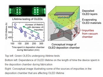
Because of these impurities in the deposition chamber, the researchers found that the time until an OLED under operation dims by a given amount because of degradation, known as the lifetime, sharply increased for OLEDs that spent a shorter time in the deposition chamber during fabrication.
This trend remained even after considering changes in residual water and source material purity, indicating the importance of controlling and minimizing the device fabrication time, a rarely discussed parameter.
Research partners at Sumika Chemical Analysis Service Ltd. (SCAS) confirmed an increase of accumulated impurities with time by analyzing the materials that deposited on extremely clean silicon wafers that were stored in the deposition chamber when OLED materials were not being evaporated.
Using a technique called liquid chromatography-mass spectrometry, the researchers found that many of the impurities could be traced to previously deposited materials and plasticizers from the vacuum chamber components.
"Really small amounts of these impurities get incorporated into the fabricated devices and are causing large changes in the lifetime," says Professor Chihaya Adachi, director of Kyushu University's Center for Organic Photonics and Electronics Research (OPERA), which also took part in the study.
In fact, the new results suggest that the impurities amount to less than even a single molecular layer.
To improve lifetime reproducibility, a practice often adopted in industry is the use of dedicated deposition chambers for specific materials, but this can be difficult in academic labs, where often only a limited number of deposition systems are available for testing a wide variety of new materials.
In these cases, deposition chamber design and cleaning in addition to control of the deposition time are especially important.
"This is an excellent reminder of just how careful we need to be to do good, reproducible science," comments Professor Adachi.
Share on:


Suggested Items
Material Insight: The Dielectric Constant of PCB Materials
05/17/2024 | Dr. Preeya Kuray -- Column: Material InsightIn the world of PCB design, miniaturization can be achieved by using low dielectric constant (Dk) materials. Low Dk materials can allow for a reduction in thickness while maintaining a given trace width, leading to lower transmission loss and higher density circuitry.
IPC APEX EXPO: Some Thoughts About Growth
05/16/2024 | Dan Feinberg, I-Connect007After two and a half days of wandering the aisles at IPC APEX EXPO 2024, for the first time, I almost felt like I was exploring CES. There were so many booths and exhibits that I could describe, but I’d like to focus on the growth and huge value of this event, which has expanded well beyond just the growing and impressive exhibit show floor.
The Shaughnessy Report: Unlock Your High-speed Material Constraints
05/15/2024 | Andy Shaughnessy -- Column: The Shaughnessy ReportThe world of PCB materials used to be a fairly simple one. It was divided into two groups: the “traditional” laminates, often called FR-4, and the high-speed laminates developed especially for high-speed PCBs. These were two worlds that usually didn’t collide. But then traditional laminates started getting better, and high-speed designers and design engineers took notice and started to reconsider what FR-4 could be used for.
Breaking High-speed Material Constraints: Design007 Magazine — May 2024
05/14/2024 | I-Connect007 Editorial TeamDo you need specialty materials for your high-speed designs? Maybe not. Improvements in resins mean designers of high-speed boards can sometimes use traditional laminate systems instead of high-speed materials, saving time and money while streamlining the fab process. In the May 2024 issue of Design007 Magazine, our contributors explain how to avoid overconstraining your materials when working with high-speed boards.
Indium Experts to Present at Electronics in Harsh Environments SMTA Conference
05/13/2024 | Indium Corporationndium Corporation Technical Manager for Europe, Africa, and the Middle East, Karthik Vijay, will deliver a technical presentation and Indium Corporation Senior Technologist, Dr. Ronald Lasky, will deliver both a workshop and technical presentation at the Electronics in Harsh Environments SMTA Conference on May 14-16 in Copenhagen, Denmark.