


 Marcy’s Musings: The ‘Magic’ of Additive Processes
 It’s Only Common Sense: More Great Business Ideas from ‘Breaking Bad’
 Material Insight: The Dielectric Constant of PCB Materials
Compound Eyes for Industry and Smartphone
January 3, 2017 | Fraunhofer-GesellschaftEstimated reading time: 3 minutes
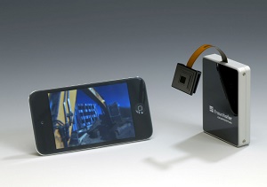
Fraunhofer researchers have developed a process enabling the production of a two millimeter flat camera. Similar to the eyes of insects, its lens is partitioned into 135 tiny facets. Following nature‘s model, the researchers have named their mini-camera concept facetVISION. At the CES technical trade fair in Las Vegas, they will be presenting it from January 5 to 8, 2017 ( LVCC Hall, South Hall 1, booth 20944).
The first prototype of the technology transfers the images from the camera to the smartphone by Bluetooth via a transmission box.
- The mini-camera from the Fraunhofer IOF has a thickness of only two milli- meters at a resolution of one megapixel.
- The cameras are therefore suitable for use in the automotive and printing industries and in medical engineering.
- Thanks to their low thickness, their basic principle may change the design of future smartphones.
The facetVISION camera can be industrially manufactured in mass production. Fraunhofer researchers have shown this in trial runs.
Just as the insects’ eyes, the Fraunhofer technology is composed of many small, uniform lenses. They are positioned close together, similar to the pieces of a mosaic. Each facet receives only a small section of its surroundings. The insect’s brain aggregates the many individual images of the facets to a whole picture. In the newly developed facetVISION camera, micro-lenses and aperture arrays take over these functions. Due to the offset of each lens to its associated aperture, each optical channel has an individual viewing direction and always depicts another area of the field of vision.
"With a camera thickness of only two millimeters, this technology, taken from nature’s model, will enable us to achieve a resolution of up to four megapixel", says Andreas Brückner, project manager at the Fraunhofer Institute for Applied Optics and Precision Engineering IOF in Jena. "This is clearly a higher resolution compared to cameras in industrial applications – for example in robot technology or automobile production." This technology was developed together with scientists from the Fraunhofer Institute for Integrated Circuits IIS in Erlangen and was funded by the Fraunhofer-Zukunftsstiftung.
Economical production on wafers
The micro-lenses of the Fraunhofer researchers can get economically manufactured in large quantities – using processes similar to those applied in the semiconductor industry. Computer chips are mass-produced on wafers (large and thin semiconductor slices) and subsequently separated by sawing. Accordingly, thousands facetVISION camera lenses can be manufactured at the Fraunhofer IOF in parallel. "The cameras are suitable in medical engineering, for instance – for optical sensors, which will be able to quickly and easily examine blood", says Brückner. "In the printing industry, however, such cameras are needed to check the print image at high resolution while the machine is running." Further applications: Cameras in cars that help parking or in industrial robots that prevent collisions between man and machines.
An eye on smartphones
Compound eye technology is also suitable for integration into smartphones: today, their mini camera lens is normally five millimeters thick in order to show a satisfactorily sharp image of the surroundings. The manufacturers of ultra-thin smarthones face the following challenge: since the camera is thicker than the smartphone housing, it sticks out of the smartphone’s back cover. The manufacturers call this the "camera-bump" – the unaesthetic "camera bulge". The camera lenses for smartphones are, however, not made on wafers, but in injection molded plastic. In this procedure, hot liquid plastic is poured into the mold in a similar way as batter into a waffle iron. Robots then assemble the finished lenses into the smartphone camera. "We would like to transfer the insect eye principle to this production technology", says Brückner. "For example, it will be possible to place several smaller lenses next to each other in the smartphone camera. The combination of facet effect and proven injection molded lenses will enable resolutions of more than 10 megapixels in a camera requiring just a thickness of around three and a half millimeters."
Share on:


Suggested Items
Marcy’s Musings: The ‘Magic’ of Additive Processes
05/21/2024 | Marcy LaRont -- Column: Marcy's MusingsThough modern semi-additive and fully additive technologies are still emerging for PCB manufacturing, additive technology itself is not new. Many PCB fabricators find themselves at a crossroads when deciding whether to change their current processes and go additive or stay the course until something significant compels a change. But change is on the horizon, and it seems to be driven by significant technological advancements in chips and advanced packaging, offering PCB fabricators some additive manufacturing solutions to explore.
Textron Systems Collaborates with Kodiak to Develop Uncrewed Military Vehicle
05/20/2024 | PRNewswireTextron Systems Corporation, a Textron Inc. company, a leading developer of crewed and uncrewed military ground vehicles, and Kodiak Robotics, Inc., a leading self-driving technology developer for the trucking and defense markets, announced that they are collaborating to develop an autonomous military ground vehicle specifically designed for driverless operations.
Additive Manufacturing: PCB007 Magazine May 2024 Issue
05/20/2024 | I-Connect007 Editorial TeamThough modern semi-additive and fully additive technologies are still emerging for PCB manufacturing, additive technology itself is not new. In this month’s issue, we explore additive manufacturing technology for the PCB fabricator: where it stands today, the true benefits, and where it seems to be headed.
Terran Orbital’s GEOStare SV2 Captures 3 Years of Success in High-Resolution Imaging
05/17/2024 | BUSINESS WIRETerran Orbital Corporation, a global leader in satellite-based solutions primarily serving the aerospace and defense industries, celebrates the 3rd anniversary of its successful GEOStare SV2 mission. Launched on May 15, 2021, from NASA’s Kennedy Space Center in Florida, GEOStare SV2 has surpassed expectations, delivering exceptional results for commercial satellite imagery.
Indium Experts to Present on High-Temperature, Lead-Free Solder Paste and High Reliability Liquid Metal Alloys Poster at ECTC
05/16/2024 | Indium CorporationIndium Corporation Research Associate Kyle Aserian will deliver a presentation at the 74th Electronic Components and Technology Conference (ECTC) on May 31, in Denver, Colorado.