


 Material Insight: The Dielectric Constant of PCB Materials
 American Made Advocacy: What About the Rest of the Technology Stack?
 It’s Only Common Sense: Great Ideas From John Mitchell’s Book on Hiring Habits
Germanium's Semiconducting and Optical Properties Probed Under Pressure
January 4, 2017 | Carnegie Institution for ScienceEstimated reading time: 2 minutes
Germanium may not be a household name like silicon, its group-mate on the periodic table, but it has great potential for use in next-generation electronics and energy technology.
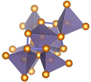
This is an illustration of ST12-germanium's complex tetragonal structure with tetrahedral bonding. (Image: Haidong Zhang)
Of particular interest are forms of germanium that can be synthesized in the lab under extreme pressure conditions. However, one of the most-promising forms of germanium for practical applications, called ST12, has only been created in tiny sample sizes--too small to definitively confirm its properties.
"Attempts to experimentally or theoretically pin down ST12-germanium's characteristics produced extremely varied results, especially in terms of its electrical conductivity," said Carnegie's Zhisheng Zhao, the first author on a new paper about this form of germanium.
The study's research team, led by Carnegie's Timothy Strobel, was able to create ST12-germanium in a large enough sample size to confirm its characteristics and useful properties. Their work is published by Nature Communications ("Properties of the exotic metastable ST12 germanium allotrope").
"This work will be of interest to a broad range of readers in the field of materials science, physics, chemistry, and engineering," explained Carnegie's Haidong Zhang, the co-leading author.
ST12-germanium has a tetragonal structure--the nameST12 means "simple tetragonal with 12 atoms." It was created by putting germanium under about 138 times normal atmospheric pressure (14 gigapascals) and then decompressing it slowly at room temperature.
The millimeter-sized samples of ST12-germanium that the team created were large enough that they could be studied using a variety of spectroscopic techniques in order to confirm its long-debated characteristics.
Like the most common, diamond-cubic form of germanium, they found that ST12 is a semiconductor with a so-called indirect band gap. Metallic substances conduct electrical current easily, whereas insulating materials conduct no current at all. Semiconducting materials exhibit mid-range electrical conductivity. When semiconducting materials are subjected to an input of a specific energy, bound electrons can be moved to higher-energy, conducting states. The specific energy required to make this jump to the conducting state is defined as the "band gap." While direct band gap materials can effectively absorb and emit light, indirect band gap materials cannot.
"Our team was able to quantify ST12's optical band gap--where visible light energy can be absorbed by the material--as well as its electrical and thermal properties, which will help define its potential for practical applications," Strobel said. "Our findings indicate that due to the size of its band gap, ST12-germanium may be a better material for infrared detection and imaging technology than the diamond-cubic form of the element already being used for these purposes."
Share on:


Suggested Items
Material Insight: The Dielectric Constant of PCB Materials
05/17/2024 | Dr. Preeya Kuray -- Column: Material InsightIn the world of PCB design, miniaturization can be achieved by using low dielectric constant (Dk) materials. Low Dk materials can allow for a reduction in thickness while maintaining a given trace width, leading to lower transmission loss and higher density circuitry.
IPC APEX EXPO: Some Thoughts About Growth
05/16/2024 | Dan Feinberg, I-Connect007After two and a half days of wandering the aisles at IPC APEX EXPO 2024, for the first time, I almost felt like I was exploring CES. There were so many booths and exhibits that I could describe, but I’d like to focus on the growth and huge value of this event, which has expanded well beyond just the growing and impressive exhibit show floor.
The Shaughnessy Report: Unlock Your High-speed Material Constraints
05/15/2024 | Andy Shaughnessy -- Column: The Shaughnessy ReportThe world of PCB materials used to be a fairly simple one. It was divided into two groups: the “traditional” laminates, often called FR-4, and the high-speed laminates developed especially for high-speed PCBs. These were two worlds that usually didn’t collide. But then traditional laminates started getting better, and high-speed designers and design engineers took notice and started to reconsider what FR-4 could be used for.
Breaking High-speed Material Constraints: Design007 Magazine — May 2024
05/14/2024 | I-Connect007 Editorial TeamDo you need specialty materials for your high-speed designs? Maybe not. Improvements in resins mean designers of high-speed boards can sometimes use traditional laminate systems instead of high-speed materials, saving time and money while streamlining the fab process. In the May 2024 issue of Design007 Magazine, our contributors explain how to avoid overconstraining your materials when working with high-speed boards.
Indium Experts to Present at Electronics in Harsh Environments SMTA Conference
05/13/2024 | Indium Corporationndium Corporation Technical Manager for Europe, Africa, and the Middle East, Karthik Vijay, will deliver a technical presentation and Indium Corporation Senior Technologist, Dr. Ronald Lasky, will deliver both a workshop and technical presentation at the Electronics in Harsh Environments SMTA Conference on May 14-16 in Copenhagen, Denmark.