


 Material Insight: The Dielectric Constant of PCB Materials
 American Made Advocacy: What About the Rest of the Technology Stack?
 It’s Only Common Sense: Great Ideas From John Mitchell’s Book on Hiring Habits
Important First Step Towards Building Electrically Pumped Nano-Lasers
January 25, 2017 | University of WashingtonEstimated reading time: 2 minutes
When an individual uses Facebook or searches Google, the information processing happens in a large data center. Short distance optical interconnects can improve the performance of these data centers. Current systems utilize electrons, which could cause overheating and wastes power. However, utilizing light to transfer information between computer chips and boards can improve efficiency.
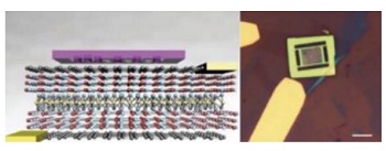
Figure 1: Schematic of the 2D material heterostructure on top of which the photonic crystal cavity is transferred. Figure 2: Optical microscope image of the cavity transferred on the 2D material heterostructure.
Assistant Professor of Electrical Engineering and Physics Arka Majumdar, Associate Professor of Materials Science and Engineering and Physics Xiaodong Xu and their team have discovered an important first step towards building electrically pumped nanolasers (or light-based sources). These lasers are critical in the development of integrated photonic based short-distance optical interconnects and sensors.
The team demonstrated this first step through cavity-enhanced electroluminescence from atomically thin monolayer materials. The thinness of this material yields efficient coordination between the two key components of the laser. Both the cavity-enhanced electroluminescence and material will allow energy-efficient data centers and support high performance parallel computing.
Recently discovered atomically thin semiconductors have generated significant interest due to showing light emission in the 2D limit. However, due to the extreme thinness of this material, its emission intensity is usually not strong enough, and it is important to integrate them with photonic devices (nano-lasers, in this case) to get more light out.
“Researchers have demonstrated electroluminescence in this material [atomically thin monolayer],” Majumdar said. “Last year, we also reported the operation of an ultra-low threshold optically pumped laser, using this material integrated with nano-cavity. But for practical applications, electrically driven devices are required. Using this, one can power the devices using electrical current. For example, you power your laser pointer using an electrical battery. ”
Majumdar and Xu recently reported cavity-enhanced electroluminescence in atomically thin material. A heterostructure of different monolayer materials are used to enhance the emission. The results were published in a recent edition of Nano Letters. Without the cavity, the emission is broadband (unidirectional) and weak. A nano-cavity enhances the emission and also enables single-mode (directed) operation. This allows direct modulation of the emission, a crucial requirement for the data-communication.
These structures are of current scientific interest and are considered the new “gold rush” of condensed matter physics and materials science. Their current result and the previous demonstration of optically pumped lasers show the promise of electrically pumped nano-lasers, which constitutes the next milestone for this research. This next achievement will improve data center efficiency for optimal performance.
“Our team is currently exploring integration of the monolayer materials with a silicon nitride platform,” Majumdar said. “Through this work, we hope to achieve the coveted CMOS [complementary metal-oxide-semiconductor] compatibility, which is the same process by which the computer processors are fabricated today.”
The research is supported by grants from the National Science Foundation and the Air Force Office of Scientific Research.
Share on:


Suggested Items
Material Insight: The Dielectric Constant of PCB Materials
05/17/2024 | Dr. Preeya Kuray -- Column: Material InsightIn the world of PCB design, miniaturization can be achieved by using low dielectric constant (Dk) materials. Low Dk materials can allow for a reduction in thickness while maintaining a given trace width, leading to lower transmission loss and higher density circuitry.
IPC APEX EXPO: Some Thoughts About Growth
05/16/2024 | Dan Feinberg, I-Connect007After two and a half days of wandering the aisles at IPC APEX EXPO 2024, for the first time, I almost felt like I was exploring CES. There were so many booths and exhibits that I could describe, but I’d like to focus on the growth and huge value of this event, which has expanded well beyond just the growing and impressive exhibit show floor.
The Shaughnessy Report: Unlock Your High-speed Material Constraints
05/15/2024 | Andy Shaughnessy -- Column: The Shaughnessy ReportThe world of PCB materials used to be a fairly simple one. It was divided into two groups: the “traditional” laminates, often called FR-4, and the high-speed laminates developed especially for high-speed PCBs. These were two worlds that usually didn’t collide. But then traditional laminates started getting better, and high-speed designers and design engineers took notice and started to reconsider what FR-4 could be used for.
Breaking High-speed Material Constraints: Design007 Magazine — May 2024
05/14/2024 | I-Connect007 Editorial TeamDo you need specialty materials for your high-speed designs? Maybe not. Improvements in resins mean designers of high-speed boards can sometimes use traditional laminate systems instead of high-speed materials, saving time and money while streamlining the fab process. In the May 2024 issue of Design007 Magazine, our contributors explain how to avoid overconstraining your materials when working with high-speed boards.
Indium Experts to Present at Electronics in Harsh Environments SMTA Conference
05/13/2024 | Indium Corporationndium Corporation Technical Manager for Europe, Africa, and the Middle East, Karthik Vijay, will deliver a technical presentation and Indium Corporation Senior Technologist, Dr. Ronald Lasky, will deliver both a workshop and technical presentation at the Electronics in Harsh Environments SMTA Conference on May 14-16 in Copenhagen, Denmark.