


 Material Insight: The Dielectric Constant of PCB Materials
 American Made Advocacy: What About the Rest of the Technology Stack?
 It’s Only Common Sense: Great Ideas From John Mitchell’s Book on Hiring Habits
Nano ‘Sandwich’ Offers Unique Properties
February 28, 2017 | Rice UniversityEstimated reading time: 2 minutes
Rice University researchers have modeled a nanoscale sandwich, the first in what they hope will become a molecular deli for materials scientists.
Their recipe puts two slices of atom-thick graphene around nanoclusters of magnesium oxide that give the super-strong, conductive material expanded optoelectronic properties.
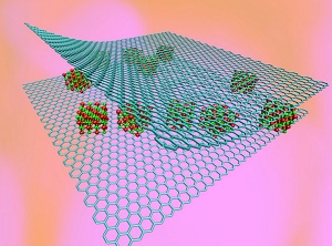
Nanoclusters of magnesium oxide sandwiched between layers of graphene make a compound with unique electronic and optical properties, according to researchers at Rice University who made computer simulations of the material.
Nanoclusters of magnesium oxide sandwiched between layers of graphene make a compound with unique electronic and optical properties, according to researchers at Rice University who made computer simulations of the material. Illustration by Lei Tao
Rice materials scientist Rouzbeh Shahsavari and his colleagues built computer simulations of the compound and found it would offer features suitable for sensitive molecular sensing, catalysis and bio-imaging. Their work could help researchers design a range of customizable hybrids of two- and three-dimensional structures with encapsulated molecules, Shahsavari said.
The scientists were inspired by experiments elsewhere in which various molecules were encapsulated using van der Waals forces to draw components together. The Rice-led study was the first to take a theoretical approach to defining the electronic and optical properties of one of those “made” samples, two-dimensional magnesium oxide in bilayer graphene, Shahsavari said.
“We knew if there was an experiment already performed, we would have a great reference point that would make it easier to verify our computations, thus allowing more reliable expansion of our computational results to identify performance trends beyond the reach of experiments,” Shahsavari said.
Graphene on its own has no band gap – the characteristic that makes a material a semiconductor. But the hybrid does, and this band gap could be tunable, depending on the components, Shahsavari said. The enhanced optical properties are also tunable and useful, he said.
“We saw that while this single flake of magnesium oxide absorbed one kind of light emission, when it was trapped between two layers of graphene, it absorbed a wide spectrum. That could be an important mechanism for sensors,” he said.
Shahsavari said his group’s theory should be applicable to other two-dimensional materials, like hexagonal boron-nitride, and molecular fillings. “There is no single material that can solve all the technical problems of the world,” he said. “It always comes down to making hybrid materials to synergize the best features of multiple components to do a specific job. My group is working on these hybrid materials by tweaking their components and structures to meet new challenges.”
Farzaneh Shayeganfar, a visiting research scientist at Rice and researcher at Shahid Rajaee Teacher Training University, Tehran, Iran, is lead author of the paper. Co-authors are Javad Beheshtiyan and Mehdi Neek-Amal, both of Shahid Rajaee and the University of Antwerp, Belgium.
Rice University and the Iran Science Elites Federation supported the research. Computing resources were supplied by Rice’s National Science Foundation-supported DAVinCI supercomputer administered by Rice’s Center for Research Computing and were procured in partnership with Rice’s Ken Kennedy Institute for Information Technology.
Share on:


Suggested Items
Material Insight: The Dielectric Constant of PCB Materials
05/17/2024 | Dr. Preeya Kuray -- Column: Material InsightIn the world of PCB design, miniaturization can be achieved by using low dielectric constant (Dk) materials. Low Dk materials can allow for a reduction in thickness while maintaining a given trace width, leading to lower transmission loss and higher density circuitry.
IPC APEX EXPO: Some Thoughts About Growth
05/16/2024 | Dan Feinberg, I-Connect007After two and a half days of wandering the aisles at IPC APEX EXPO 2024, for the first time, I almost felt like I was exploring CES. There were so many booths and exhibits that I could describe, but I’d like to focus on the growth and huge value of this event, which has expanded well beyond just the growing and impressive exhibit show floor.
The Shaughnessy Report: Unlock Your High-speed Material Constraints
05/15/2024 | Andy Shaughnessy -- Column: The Shaughnessy ReportThe world of PCB materials used to be a fairly simple one. It was divided into two groups: the “traditional” laminates, often called FR-4, and the high-speed laminates developed especially for high-speed PCBs. These were two worlds that usually didn’t collide. But then traditional laminates started getting better, and high-speed designers and design engineers took notice and started to reconsider what FR-4 could be used for.
Breaking High-speed Material Constraints: Design007 Magazine — May 2024
05/14/2024 | I-Connect007 Editorial TeamDo you need specialty materials for your high-speed designs? Maybe not. Improvements in resins mean designers of high-speed boards can sometimes use traditional laminate systems instead of high-speed materials, saving time and money while streamlining the fab process. In the May 2024 issue of Design007 Magazine, our contributors explain how to avoid overconstraining your materials when working with high-speed boards.
Indium Experts to Present at Electronics in Harsh Environments SMTA Conference
05/13/2024 | Indium Corporationndium Corporation Technical Manager for Europe, Africa, and the Middle East, Karthik Vijay, will deliver a technical presentation and Indium Corporation Senior Technologist, Dr. Ronald Lasky, will deliver both a workshop and technical presentation at the Electronics in Harsh Environments SMTA Conference on May 14-16 in Copenhagen, Denmark.