


 The Right Approach: I Hear the Train A Comin'
 It’s Only Common Sense: OCCAM—the Time Is Now
 Marcy's Musings: The Growing Industry
Towards Super-Efficient, Ultra-Thin Silicon Solar Cells
March 22, 2017 | NERSCEstimated reading time: 4 minutes
Despite a surge in solar cell R&D in recent years involving emerging materials such as organics and perovskites, the solar cell industry continues to favor inorganic crystalline silicon photovoltaics. While thin-film solar cells offer several advantages—including lower manufacturing costs—long-term stability of crystalline silicon solar cells, which are typically thicker, tips the scale in their favor, according to Rana Biswas, a senior scientist at Ames Laboratory, who has been studying solar cell materials and architectures for two decades.
“Crystalline silicon solar cells today account for more than 90% of all installations worldwide,” said Biswas, co-author of a new study that used supercomputers at Berkeley Lab’s National Energy Research Scientific Computing Center (NERSC), a Department of Energy Office of Science User Facility, to evaluate a novel approach for creating more energy-efficient ultra-thin crystalline silicon solar cells. “The industry is very skeptical that any other material could be as stable as silicon.”
Thin-film solar cells typically fabricated from semiconductor materials such as amorphous silicon are only a micron thick. While this makes them less expensive to manufacture than crystalline silicon solar cells, which are around 180 microns thick, it also makes them less efficient—12% to 14% energy conversion, versus nearly 25% for silicon solar cells (which translates into 15-21% for large area panels, depending on the size). This is because if the wavelength of incoming light is longer than the solar cell is thick, the light won’t be absorbed.
Nanocone Arrays
This challenge prompted Biswas and colleagues at Ames to look for ways to improve ultra-thin silicon cell architectures and efficiencies. In a paper published in Nanomaterials, they describe their efforts to develop a highly absorbing ultra-thin crystalline silicon solar cell architecture with enhanced light trapping capabilities.
“We were able to design a solar cell with a very thin amount of silicon that could still provide high performance, almost as high performance as the thick silicon being used today,” Biswas said.
Nanomaterials
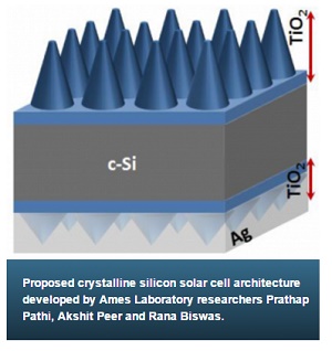
Proposed crystalline silicon solar cell architecture developed by Ames Laboratory researchers Prathap Pathi, Akshit Peer and Rana Biswas.
The key lies in the wavelength of light that is trapped and the nanocone arrays used to trap it. Their proposed solar architecture comprises thin flat spacer titanium dioxide layers on the front and rear surfaces of silicon, nanocone gratings on both sides with optimized pitch and height and rear cones surrounded by a metallic reflector made of silver. They then set up a scattering matrix code to simulate light passing through the different layers and study how the light is reflected and transmitted at different wavelengths by each layer.
“This is a light-trapping approach that keeps the light, especially the red and long-wavelength infrared light, trapped within the crystalline silicon cell,” Biswas explained. “We did something similar to this with our amorphous silicon cells, but crystalline behaves a little differently.”
For example, it is critical not to affect the crystalline silicon wafer—the interface of the wafer—in any way, he emphasized. “You want the interface to be completely flat to begin with, then work around that when building the solar cell,” he said. “If you try to pattern it in some way, it will introduce a lot of defects at the interface, which are not good for solar cells. So our approach ensures we don’t disturb that in any way.”
Homegrown Code
In addition to the cell’s unique architecture, the simulations the researchers ran on NERSC’s Edison system utilized “homegrown” code developed at Ames to model the light via the cell’s electric and magnetic fields—a “classical physics approach,” Biswas noted. This allowed them to test multiple wavelengths to determine which was most optimum for light trapping. To optimize the absorption of light by the crystalline silicon based upon the wavelength, the team sent light waves of different wavelengths into a designed solar cell and then calculated the absorption of light in that solar cell’s architecture. The Ames researchers had previously studied the trapping of light in other thin film solar cells made of organic and amorphous silicon in previous studies.
“One very nice thing about NERSC is that once you set up the problem for light, you can actually send each incoming light wavelength to a different processor (in the supercomputer),” Biswas said. “We were typically using 128 or 256 wavelengths and could send each of them to a separate processor.”
Looking ahead, given that this research is focused on crystalline silicon solar cells, this new design could make its way into the commercial sector in the not-too-distant future—although manufacturing scalability could pose some initial challenges, Biswas noted.
“It is possible to do this in a rather inexpensive way using soft lithography or nanoimprint lithography processes,” he said. “It is not that much work, but you need to set up a template or a master to do that. In terms of real-world applications, these panels are quite large, so that is a challenge to do something like this over such a large area. But we are working with some groups that have the ability to do roll to roll processing, which would be something they could get into more easily.”
About NERSC and Berkeley Lab
The National Energy Research Scientific Computing Center (NERSC) is a U.S. Department of Energy Office of Science User Facility that serves as the primary high-performance computing center for scientific research sponsored by the Office of Science. Located at Lawrence Berkeley National Laboratory, the NERSC Center serves more than 6,000 scientists at national laboratories and universities researching a wide range of problems in combustion, climate modeling, fusion energy, materials science, physics, chemistry, computational biology, and other disciplines. Berkeley Lab is a DOE national laboratory located in Berkeley, California. It conducts unclassified scientific research and is managed by the University of California for the U.S. DOE Office of Science. »Learn more about computing sciences at Berkeley Lab.
Share on:


Suggested Items
Real Time with... IPC APEX EXPO 2024: Sustainability in the Industry
04/26/2024 | Real Time with...IPC APEX EXPOGuest Editor Henry Crandall and Chris Nash of Indium Corporation discuss the company's 90th anniversary and its focus on sustainability. They focus on the benefits of sustainable materials, their compatibility, and value propositions. The conversation also highlights how Durafuse LT technology's role in reducing reflow temperatures is leading to significant cost and energy savings. Nash also touches on downstream sustainability efforts such as using recycled materials for packaging.
Fujitsu, METRON Collaborate to Drive ESG Success
04/24/2024 | JCN NewswireFujitsu Limited and METRON SAS, a French cleantech company specializing in energy management solutions for industrial decarbonization, today announced a strategic initiative to contribute to the realization of carbon neutrality in the manufacturing industry.
Amphenol Corporation Releases 2023 Sustainability Report
04/23/2024 | Amphenol CorporationAmphenol Corporation released its 2023 Sustainability Report.
Foxconn Pledges 100% Renewable Electricity by 2040, Joins RE100
04/22/2024 | FoxconnHon Hai Technology Group announced its worldwide operations will run fully on green electricity by 2040 and has joined the global initiative RE100, in a milestone on Earth Day 2024 that adds the world’s largest electronics manufacturer and technology solution provider among the most influential businesses committed to 100% renewable electricity.
Altus Group Helps BitBox Unlock Productivity and Efficiency Gains with New Reflow Oven
04/22/2024 | Altus GroupAltus Group, a leading provider of capital equipment, has recently assisted BitBox, a UK-based electronics design, engineering and manufacturing company in upgrading its operations with the implementation of a new reflow oven from Heller Industries.