


 The Chemical Connection: Reducing Etch System Water Usage, Part 2
 It’s Only Common Sense: Nice Guys Really Can Finish First
 The Right Approach: I Hear the Train A Comin'
Seeing The Invisible With A Graphene-CMOS Integrated Device
June 6, 2017 | Graphene FlagshipEstimated reading time: 2 minutes
Silicon based CMOS (Complementary metal-oxide semiconductors) technology has truly shaped our world. It enables most of the electronics that we rely on today including computers, smartphones and digital cameras. However, to continue the path of progress in the electronics industry new technology must be developed and a key feature of this is the ability to integrate CMOS with other semiconductors. Now, Graphene Flagship researchers from ICFO (The Institute of Photonic Sciences in Barcelona) have shown that it is possible to integrate graphene into a CMOS integrated circuit.
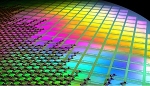
Flagship researchers integrate graphene and quantum dots with CMOS technology to create an array of photodetectors, producing a high resolution image sensor. Image Credit: Fabien Vialla
In their paper published in the journal Nature Photonics they combine this graphene-CMOS device with quantum dots to create an array of photodetectors, producing a high resolution image sensor. When used as a digital camera this device is able to sense UV, visible and infrared light at the same time. This is just one example of how this device might be used, others include in microelectronics, sensor arrays and low-power photonics.
“The development of this monolithic CMOS-based image sensor represents a milestone for low-cost, high-resolution broadband and hyperspectral imaging systems” ICREA Professor at ICFO, Frank Koppens, highlights. He assures that “in general, graphene-CMOS technology will enable a vast amount of applications, that range from safety, security, low cost pocket and smartphone cameras, fire control systems, passive night vision and night surveillance cameras, automotive sensor systems, medical imaging applications, food and pharmaceutical inspection to environmental monitoring, to name a few”.
These results were enabled by the collaboration between Graphene Flagship Partner Graphenea (a Spanish graphene supplier) and ICFO, within the optoelectronics workpackage of the Graphene Flagship.
By creating a hybrid graphene and quantum dot system on a CMOS wafer using a layering and patterning approach, the Flagship team solved a complex problem with a simple solution. First the graphene is deposited, then patterned to define the pixel shape and finally a layer of PbS colloidal quantum dots is added. The photoresponse of this system is based on a photogating effect, which starts as the quantum dot layer absorbs light and transfers it as photo-generated holes or electrons to the graphene, where they circulate due to a bias voltage applied between two pixel contacts. The photo signal is then sensed by the change in conductivity of the graphene, with graphene’s high charge mobility allowing for the high sensitivity of the device.
As Stijn Goossens comments, “No complex material processing or growth processes were required to achieve this graphene-quantum dot CMOS image sensor. It proved easy and cheap to fabricate at room temperature and under ambient conditions, which signifies a considerable decrease in production costs. Even more, because of its properties, it can be easily integrated on flexible substrates as well as CMOS-type integrated circuits.”
The commercial applications of this research and the potential for imaging and sensing technology are now being explored in ICFO’s Launchpad incubator.
Professor Andrea Ferrari, Science and Technology Officer and Chair of the Management Panel of the Graphene Flagship added: "The integration of graphene with CMOS technology is a cornerstone for the future implementation of graphene in consumer electronics. This work is a key first step, clearly demonstrating the feasibility of this approach. The Flagship has put a significant investment in the system level integration of graphene, and this will increase as we move along the technology and innovation roadmap".
Click here for the original article.
Share on:


Suggested Items
iNEMI Names Grace O'Malley CTO
05/02/2024 | iNEMIThe Board of Directors of the International Electronics Manufacturing Initiative (iNEMI) has named Grace O'Malley Chief Technical Officer (CTO).
Dubai Launches Global Blueprint for Artificial Intelligence
05/02/2024 | BUSINESS WIREDubai has launched a blueprint for Artificial Intelligence (AI), a yearly plan that will focus on harnessing the technology’s potential to improve quality of life around the world.
NextFlex Convenes the Hybrid Electronics Community at Binghamton University
05/01/2024 | NextFlexBinghamton University hosted the NextFlex hybrid electronics community on April 18 for a day of expert presentations, breakout sessions on technology and manufacturing topics, and networking.
IDTechEx Report on Quantum Technology: Nano-scale Physics for Massive Market Impact
04/30/2024 | PRNewswireThe quantum technology market leverages nano-scale physics to create revolutionary new devices for computing, sensing, and communications. Across the industry, quantum technology offers a paradigm shift in performance compared with incumbent solutions.
TSMC Certifies Ansys Multiphysics Platforms, Enabling Next-Gen AI and HPC Chips
04/30/2024 | PRNewswireAnsys announced the certification of its power integrity platforms for TSMC's N2 technology full production release. Both Ansys RedHawk-SC and Ansys Totem are certified for power integrity signoff on the N2 process, delivering significant speed and power advantages for high performance computing, mobile chips, and 3D-IC designs.