


 The Right Approach: I Hear the Train A Comin'
 It’s Only Common Sense: OCCAM—the Time Is Now
 Marcy's Musings: The Growing Industry
Laying the Foundations for Hybrid Silicon Lasers
June 16, 2017 | A*STAREstimated reading time: 2 minutes
Producing semiconductor lasers on a silicon wafer is a long-held goal for the electronics industry, but their fabrication has proved challenging. Now, researchers at A*STAR have developed an innovative way to manufacture them that is cheap, simple and scalable.
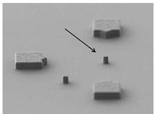
Oblique angle scanning electron microscopy image of a 500 nanometer diameter microdisk.
Hybrid silicon lasers combine the light-emitting properties of group III–V semiconductors, like gallium arsenide and indium phosphide, with the maturity of silicon manufacturing techniques. These lasers are attracting considerable attention as they promise inexpensive, mass-producible optical devices that can integrate with photonic and microelectronic elements on a single silicon chip. They have potential in a wide range of applications, from short-distance data communication to high-speed, long-distance optical transmission.
In the current production process, however, lasers are fabricated on separate III–V semiconductor wafers before being individually aligned to each silicon device — a time-consuming, costly process that limits the number of lasers that can be placed on a chip.
To overcome these limitations, Doris Keh-Ting Ng and her colleagues from the A*STAR Data Storage Institute have developed an innovative method for producing a hybrid III–V semiconductor and silicon-on-insulator (SOI) optical microcavity. This greatly reduces the complexity of the fabrication process and results in a more compact device.
“It’s very challenging to etch the entire cavity,” says Ng. “Currently, there is no single etch recipe and mask that allows the whole microcavity to be etched, and so we decided to develop a new approach.”
By first attaching a thin film of III–V semiconductor to a silicon oxide (SiO2) wafer using a SOI interlayer thermal bonding process, they produced a strong bond that also removes the need for strong oxidizing agents, such as Piranha solution or hydrofluoric acid.
And by using a dual hard-mask technique to etch the microcavity that confined etching to the intended layer, they eliminated the requirement to use multiple overlay lithography and etching cycles — a challenging procedure.
“Our approach cuts down the number of fabrication steps, reduces the use of hazardous chemicals, and requires only one lithography step to complete the process,” explains Ng.
The work presents, for the first time, a new heterocore configuration and integrated fabrication process that combines low-temperature SiO2 interlayer bonding with dual hard-mask, single lithography patterning.
“The process not only makes it possible to produce heterocore devices, it also greatly reduces the challenges of fabricating them, and could serve as an alternative hybrid microcavity for use by the research community,” says Ng.
Share on:


Suggested Items
Koh Young Showcases Award-winning Inspection Solutions at SMTconnect with SmartRep in Hall 4A.225
04/25/2024 | Koh Young TechnologyKoh Young Technology, the industry leader in True 3D measurement-based inspection solutions, will showcase an array of award-winning inspection and measurement solutions at SMTconnect alongside its sales partner, SmartRep, in booth 4A.225 at NürnbergMesse from June 11-13, 2023. The following offers a glimpse into what Koh Young will present at the tradeshow:
Real Time with… IPC APEX EXPO 2024: Plasmatreat: Innovative Surface Preparation Solutions
04/25/2024 | Real Time with...IPC APEX EXPOIn this interview, Editor Nolan Johnson speaks with Hardev Grewal, CEO and president of Plasmatreat, a developer of atmospheric plasma solutions. Plasmatreat uses clean compressed air and electricity to create plasma, offering environmentally friendly methods for surface preparation. Their technology measures plasma density for process optimization and can remove organic micro-contamination. Nolan and Hardev also discuss REDOX-Tool, a new technology for removing metal oxides.
KYZEN to Promote Pair of Stencil Cleaning Chemistries at SMTA Ciudad Jaurez Expo & Tech Forum
04/25/2024 | KYZEN'KYZEN, the global leader in innovative environmentally friendly cleaning chemistries, will exhibit at the SMTA Ciudad Juarez Expo & Tech Forum, scheduled to take place Thursday, May 9, 2024 at the Injectronic Convention Center in Ciudad Jaurez, Chihuahua, Mexico. During the event the KYZEN Clean Team will focus on understencil cleaning products KYZEN E5631J and CYBERSOLV C8882.
Cadence, TSMC Collaborate on Wide-Ranging Innovations to Transform System and Semiconductor Design
04/25/2024 | Cadence Design SystemsCadence Design Systems, Inc. and TSMC have extended their longstanding collaboration by announcing a broad range of innovative technology advancements to accelerate design, including developments ranging from 3D-IC and advanced process nodes to design IP and photonics.
Listen Up! The Intricacies of PCB Drilling Detailed in New Podcast Episode
04/25/2024 | I-Connect007In episode 5 of the podcast series, On the Line With: Designing for Reality, Nolan Johnson and Matt Stevenson continue down the manufacturing process, this time focusing on the post-lamination drilling process for PCBs. Matt and Nolan delve into the intricacies of the PCB drilling process, highlighting the importance of hole quality, drill parameters, and design optimization to ensure smooth manufacturing. The conversation covers topics such as drill bit sizes, aspect ratios, vias, challenges in drilling, and ways to enhance efficiency in the drilling department.