


 Material Insight: The Dielectric Constant of PCB Materials
 American Made Advocacy: What About the Rest of the Technology Stack?
 It’s Only Common Sense: Great Ideas From John Mitchell’s Book on Hiring Habits
Nanostructures Detect Colors
June 30, 2017 | CaltechEstimated reading time: 3 minutes
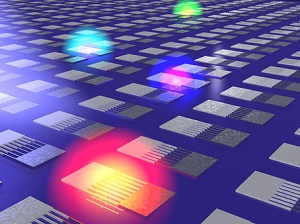
Engineers at Caltech have for the first time developed a light detector that combines two disparate technologies—nanophotonics, which manipulates light at the nanoscale, and thermoelectrics, which translates temperature differences directly into electron voltage—to distinguish different wavelengths of light, including both visible and infrared wavelengths, at high resolution.
Light detectors that distinguish between different colors of light or heat are used in a variety of applications, including satellites that study changing vegetation and landscape on the earth and medical imagers that distinguish between healthy and cancerous cells based on their color variations.
The new detector, described in a paper in Nature Nanotechnology on May 22, operates about 10 to 100 times faster than current comparable thermoelectric devices and is capable of detecting light across a wider range of the electromagnetic spectrum than traditional light detectors. In traditional light detectors, incoming photons of light are absorbed in a semiconductor and excite electrons that are captured by the detector. The movement of these light-excited electrons produces an electric current—a signal—that can be measured and quantified. While effective, this type of system makes it difficult to "see" infrared light, which is made up of lower-energy photons than those in visible light.
Because the new detectors are potentially capable of capturing infrared wavelengths of sunlight and heat that cannot be collected efficiently by conventional solar materials, the technology could lead to better solar cells and imaging devices.
"In nanophotonics, we study the way light interacts with structures that are much smaller than the optical wavelength itself, which results in extreme confinement of light. In this work, we have combined this attribute with the power conversion characteristics of thermoelectrics to enable a new type of optoelectronic device," says Harry Atwater, corresponding author of the study. Atwater is the Howard Hughes Professor of Applied Physics and Materials Science in the Division of Engineering and Applied Science at Caltech, and director of the Joint Center for Artificial Photosynthesis (JCAP). JCAP is a Department of Energy (DOE) Energy Innovation Hub focused on developing a cost-effective method of turning sunlight, water, and carbon dioxide into fuel. It is led by Caltech with Berkeley Lab as a major partner.
Atwater's team built materials with nanostructures that are hundreds of nanometers wide—smaller even than the wavelengths of light that represent the visible spectrum, which ranges from about 400 to 700 nanometers.
The researchers created nanostructures with a variety of widths, that absorb different wavelengths—colors—of light. When these nanostructures absorb light, they generate an electric current with a strength that corresponds to the light wavelength that is absorbed.
The detectors were fabricated in the Kavli Nanoscience Institute cleanroom at Caltech, where the team created subwavelength structures using a combination of vapor deposition (which condenses atom-thin layers of material on a surface from an element-rich mist) and electron beam lithography (which then cuts nanoscale patterns in that material using a focused beam of electrons). The structures, which resonate and generate a signal when they absorb photons with specific wavelengths, were created from alloys with well-known thermoelectric properties, but the research is applicable to a wide range of materials, the authors say.
"This research is a bridge between two research fields, nanophotonics and thermoelectrics, that don't often interact, and creates an avenue for collaboration," says graduate student Kelly Mauser (MS '16), lead author of the Nature Nanotechnology study. "There is a plethora of unexplored and exciting application and research opportunities at the junction of these two fields."
Share on:


Suggested Items
Material Insight: The Dielectric Constant of PCB Materials
05/17/2024 | Dr. Preeya Kuray -- Column: Material InsightIn the world of PCB design, miniaturization can be achieved by using low dielectric constant (Dk) materials. Low Dk materials can allow for a reduction in thickness while maintaining a given trace width, leading to lower transmission loss and higher density circuitry.
IPC APEX EXPO: Some Thoughts About Growth
05/16/2024 | Dan Feinberg, I-Connect007After two and a half days of wandering the aisles at IPC APEX EXPO 2024, for the first time, I almost felt like I was exploring CES. There were so many booths and exhibits that I could describe, but I’d like to focus on the growth and huge value of this event, which has expanded well beyond just the growing and impressive exhibit show floor.
The Shaughnessy Report: Unlock Your High-speed Material Constraints
05/15/2024 | Andy Shaughnessy -- Column: The Shaughnessy ReportThe world of PCB materials used to be a fairly simple one. It was divided into two groups: the “traditional” laminates, often called FR-4, and the high-speed laminates developed especially for high-speed PCBs. These were two worlds that usually didn’t collide. But then traditional laminates started getting better, and high-speed designers and design engineers took notice and started to reconsider what FR-4 could be used for.
Breaking High-speed Material Constraints: Design007 Magazine — May 2024
05/14/2024 | I-Connect007 Editorial TeamDo you need specialty materials for your high-speed designs? Maybe not. Improvements in resins mean designers of high-speed boards can sometimes use traditional laminate systems instead of high-speed materials, saving time and money while streamlining the fab process. In the May 2024 issue of Design007 Magazine, our contributors explain how to avoid overconstraining your materials when working with high-speed boards.
Indium Experts to Present at Electronics in Harsh Environments SMTA Conference
05/13/2024 | Indium Corporationndium Corporation Technical Manager for Europe, Africa, and the Middle East, Karthik Vijay, will deliver a technical presentation and Indium Corporation Senior Technologist, Dr. Ronald Lasky, will deliver both a workshop and technical presentation at the Electronics in Harsh Environments SMTA Conference on May 14-16 in Copenhagen, Denmark.