


 It’s Only Common Sense: Nice Guys Really Can Finish First
 The Right Approach: I Hear the Train A Comin'
 Marcy's Musings: The Growing Industry
Nanoparticles Could Spur Better LEDs, Invisibility Cloaks
July 20, 2017 | University of MichiganEstimated reading time: 4 minutes
In an advance that could boost the efficiency of LED lighting by 50% and even pave the way for invisibility cloaking devices, a team of University of Michigan researchers has developed a new technique that peppers metallic nanoparticles into semiconductors.
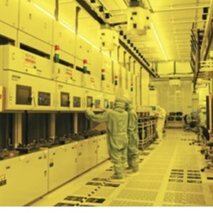
The inside of the main concourse of the molecular beam epitaxy apparatus, which University of Michigan engineering researchers used to make the advanced nanoparticle-infused gallium nitride semiconductors. The semiconductors could boost LED efficiency by up to 50%, and even lead to invisibility cloaking devices. Image credit: Joseph Xu, Michigan Engineering
It's the first technique that can inexpensively grow metal nanoparticles both on and below the surface of semiconductors. The process adds virtually no cost during manufacturing and its improved efficiency could allow manufacturers to use fewer semiconductors in finished products, making them less expensive.
The metal nanoparticles can increase the efficiency of LEDs in several ways. They can act as tiny antennas that alter and redirect the electricity running through the semiconductor, turning more of it into light. They can also help reflect light out of the device, preventing it from being trapped inside and wasted.
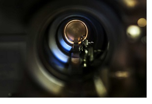
The main growth chamber of the molecular epitaxy beam apparatus used to make the nanoparticle-infused gallium nitride semiconductors. The semiconductors could boost LED efficiency by up to 50 percent, and even lead to invisibility cloaking devices. Image credit: Joseph Xu, Michigan Engineering
The process can be used with the gallium nitride that's used in LED lighting and can also boost efficiency in other semiconductor products, including solar cells. It's detailed in a study published in the Journal of Applied Physics.
"This is a seamless addition to the manufacturing process, and that's what makes it so exciting," said Rachel Goldman, U-M professor of materials science and engineering, and physics. "The ability to make 3-D structures with these nanoparticles throughout is going to open a lot of possibilities."
The key innovation
The idea of adding nanoparticles to increase LED efficiency is not new. But previous efforts to incorporate them have been impractical for large-scale manufacturing. They focused on pricey metals like silver, gold and platinum. In addition, the size and spacing of the particles must be very precise; this required additional and expensive manufacturing steps. Furthermore, there was no cost-effective way to incorporate particles below the surface.
Former materials science PhD student Sunyeol Jun prepares the molecular beam epitaxy apparatus that’s used to make the nanoparticle-infused gallium nitride semiconductors. The semiconductors could boost LED efficiency by up to 50%, and even lead to invisibility cloaking devices. Image credit: Joseph Xu, Michigan Engineering
Goldman's team discovered a simpler way that integrates easily with the molecular beam epitaxy process used to make semiconductors. Molecular beam epitaxy sprays multiple layers of metallic elements onto a wafer. This creates exactly the right conductive properties for a given purpose.
The U-M researchers applied an ion beam between these layers—a step that pushes metal out of the semiconductor wafer and onto the surface. The metal forms nanoscale particles that serve the same purpose as the pricey gold and platinum flecks in earlier research. Their size and placement can be precisely controlled by varying the angle and intensity of the ion beam. And applying the ion beam over and over between each layer creates a semiconductor with the nanoparticles interspersed throughout.
"If you carefully tailor the size and spacing of nanoparticles and how deeply they're embedded, you can find a sweet spot that enhances light emissions," said Myungkoo Kang, a former graduate student in Goldman's lab and first author on the study. "This process gives us a much simpler and less expensive way to do that."
A microscopy photo showing an array of precisely placed metallic nanoparticles on the surface of a gallium arsenide semiconductor. Image courtesy: Rachel S. Goldman, Michigan Engineering
Researchers have known for years that metallic particles can collect on the surface of semiconductors during manufacturing. But they were always considered a nuisance, something that happened when the mix of elements was incorrect or the timing was off.
"From the very early days of semiconductor manufacturing, the goal was always to spray a smooth layer of elements onto the surface. If the elements formed particles instead, it was considered a mistake," Goldman said. "But we realized that those 'mistakes' are very similar to the particles that manufacturers have been trying so hard to incorporate into LEDs. So, we figured out a way to make lemonade out of lemons."
Toward invisibility cloaks
Because the technique allows precise control over the nanoparticle distribution, the researchers say it may one day be useful for cloaks that render objects partially invisible by inducing a phenomenon known as "reverse refraction."
Reverse refraction bends light waves backwards in a way that doesn't occur in nature, potentially directing them around an object or away from the eye. The researchers believe that by carefully sizing and spacing an array of nanoparticles, they may be able to induce and control reverse refraction in specific wavelengths of light.
"For invisibility cloaking, we need to both transmit and manipulate light in very precise ways, and that's very difficult today," Goldman said. "We believe that this process could give us the level of control we need to make it work."
The team is now working to adapt the ion beam process to the specific materials used in LEDs—they estimate that the higher-efficiency lighting devices could be ready for market within the next five years, with invisibility cloaking and other applications coming further in the future.
The study is titled "Formation of embedded plasmonic Ga nanoparticle arrays and their influence on GaAs photoluminescence." The research was supported by the National Science Foundation through the Materials Research Science and Engineering Center at U-M.
Share on:


Suggested Items
The Knowledge Base: A CM’s Perspective on Box Build Practices
04/30/2024 | Mike Konrad -- Column: The Knowledge BaseIn the ever-evolving landscape of electronics manufacturing, the box-build process stands out as a critical phase that bridges the gap between individual component manufacturing and the delivery of a fully functional electronic system. This intricate procedure, encompassing the assembly of everything from PCBs to wire harnesses and mechanical enclosures, demands a high level of precision, efficiency, and innovation. As the electronics assembly industry expands and diversifies, understanding the best practices within box-build assembly has become paramount for manufacturers aiming to stay ahead in a competitive market.
TSMC Certifies Ansys Multiphysics Platforms, Enabling Next-Gen AI and HPC Chips
04/30/2024 | PRNewswireAnsys announced the certification of its power integrity platforms for TSMC's N2 technology full production release. Both Ansys RedHawk-SC and Ansys Totem are certified for power integrity signoff on the N2 process, delivering significant speed and power advantages for high performance computing, mobile chips, and 3D-IC designs.
Koh Young Showcases Award-winning Inspection Solutions at SMTconnect with SmartRep in Hall 4A.225
04/25/2024 | Koh Young TechnologyKoh Young Technology, the industry leader in True 3D measurement-based inspection solutions, will showcase an array of award-winning inspection and measurement solutions at SMTconnect alongside its sales partner, SmartRep, in booth 4A.225 at NürnbergMesse from June 11-13, 2023. The following offers a glimpse into what Koh Young will present at the tradeshow:
Real Time with… IPC APEX EXPO 2024: Plasmatreat: Innovative Surface Preparation Solutions
04/25/2024 | Real Time with...IPC APEX EXPOIn this interview, Editor Nolan Johnson speaks with Hardev Grewal, CEO and president of Plasmatreat, a developer of atmospheric plasma solutions. Plasmatreat uses clean compressed air and electricity to create plasma, offering environmentally friendly methods for surface preparation. Their technology measures plasma density for process optimization and can remove organic micro-contamination. Nolan and Hardev also discuss REDOX-Tool, a new technology for removing metal oxides.
KYZEN to Promote Pair of Stencil Cleaning Chemistries at SMTA Ciudad Jaurez Expo & Tech Forum
04/25/2024 | KYZEN'KYZEN, the global leader in innovative environmentally friendly cleaning chemistries, will exhibit at the SMTA Ciudad Juarez Expo & Tech Forum, scheduled to take place Thursday, May 9, 2024 at the Injectronic Convention Center in Ciudad Jaurez, Chihuahua, Mexico. During the event the KYZEN Clean Team will focus on understencil cleaning products KYZEN E5631J and CYBERSOLV C8882.