-

- News
- Books
Featured Books
- smt007 Magazine
Latest Issues
Current Issue
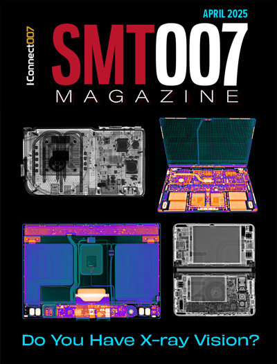
Do You Have X-ray Vision?
Has X-ray’s time finally come in electronics manufacturing? Join us in this issue of SMT007 Magazine, where we answer this question and others to bring more efficiency to your bottom line.

IPC APEX EXPO 2025: A Preview
It’s that time again. If you’re going to Anaheim for IPC APEX EXPO 2025, we’ll see you there. In the meantime, consider this issue of SMT007 Magazine to be your golden ticket to planning the show.

Technical Resources
Key industry organizations–all with knowledge sharing as a part of their mission–share their technical repositories in this issue of SMT007 Magazine. Where can you find information critical to your work? Odds are, right here.
- Articles
- Columns
Search Console
- Links
- Media kit
||| MENU - smt007 Magazine
Process Step Elimination: Driven by Cost and Efficiency, Enabled by Process and Materials Innovation
August 8, 2017 | Westin Bent, Alpha Assembly SolutionsEstimated reading time: 3 minutes
Electronics manufacturing has evolved from the early days of hand soldering and wave soldering to the more modern surface mount technology (SMT) process. Most modern electronics are produced using the SMT process, but there are still some mixed technology applications, such as assemblies that are produced using both the SMT process and the wave soldering process.
The number of mixed technology assemblies has decreased over time due to advances in the SMT process and the cost savings and increased efficiencies associated with eliminating the wave soldering process.
The recent electronics industry transition from SnPb-based alloys to lead-free alloys has provided electronics manufacturers with the incentive to try to eliminate the wave soldering process step due to the following:
- Need for equipment upgrades in order to process new lead-free alloys
- Higher energy costs due to the higher processing temperatures of the lead-free alloys
- Higher material costs associated with lead-free alloys
- Increased efficiency associated with eliminating an additional process step
- Ability to avoid exposing the assembly to the additional thermal stresses introduced by the wave soldering process
Advances in the SMT process such as the development of the pin-in-paste (PiP) process, has enabled the soldering of through-hole components during SMT processing, eliminating the need for the wave process. In the pin-in-paste process, the solder paste is first printed directly on top of the through-holes on the circuit board. The through-hole component pins are then inserted into the solder paste, and completely through the through-holes. Solder materials suppliers have been instrumental in making these process advances viable by developing solder pastes with rheological properties optimized for this type of processing, increasing process yields and reducing issues such as paste dripping from the pins as the assembly moves down the SMT line, particularly in the reflow oven.
Solder material suppliers have also been proactive in developing materials and process solutions to some of the challenges that are inherent to the PiP process. One such challenge is the need to provide enough solder volume to completely fill the through-hole providing the required mechanical and electrical reliability. In many cases, due to restricted real estate on the surface of the circuit board and the intricacies of component design, it is not possible to overprint with enough solder paste (which is only about 50% solder metal to begin with) to completely fill the through-hole, especially on the inner rows of a fine pitch connector.
As board thickness increases, it becomes even more challenging to provide enough solder to fill the through-hole. One solution that has been developed that eliminates the need for a step stencil, is the use of solder preforms to provide the additional solder to the joint. Solder preforms can be stamped in various shapes from solder ribbon and are pure metal alloy.
The volume of solder required to fill a through-hole can be calculated and the appropriate sized preform can be stamped to provide enough solder to fill the through-hole. Preforms packaged in tape and reel can then be fed into pick and place equipment to be automatically placed in the appropriate locations.
Flux-coated preforms are also increasingly being utilized as part of a voiding mitigation strategy for certain die attach and bottom termination component (BTC) soldering applications where thermal management is critical. Void reduction in these joints means increased thermal conduction away from the die resulting in better die performance and longer lifetimes. Recent studies have shown that flux coated preforms used in conjunction with solder paste can give voiding levels below 5% on BTC components.1 In some die attach applications, flux coated preforms can be used in conjunction with dispensed paste flux, totally eliminating the need to print solder paste. Pick and place equipment is also now available on the market where dispensing of solder paste or flux material and component mounting can be alternately performed. This means that no separate dispensing equipment would be needed for such a process.
In the case of die attach and BTC soldering applications, the drivers leading to process elimination are improved product reliability and improved assembly process yields, but these are only made possible due to the materials and process development work done by solder materials suppliers.
References
1. Lifton, Anna; Sidone, Jerry; Salerno, Paul; Khaselev, Oscar; Marzi, Mike;. s.l. Void Reduction Strategy for Bottom Termination Components (BTC) Using Flux Coated Preforms. SMTAi 2017.
This article was originally published in the August 2017 issue of SMT Magazine.
Suggested Items
KOKI Expands U.S. Sales Coverage with Multiple New Representatives
04/29/2025 | KOKIKOKI, a global leader in advanced soldering materials and process optimization services, is pleased to announce the expansion of its U.S. sales network with the addition of three new manufacturers’ representative firms: Assembled Product Specialists, Diversitech Reps Inc., and Eagle Electronics.
INEMI Call-for-Participation Webinar: BiSn-Based Low-Temperature Soldering Process and Reliability Project Phase 3b
04/28/2025 | iNEMIIn 2015, INEMI initiated the BiSn-Based Low-Temperature Soldering Process and Reliability Project to assess the feasibility of using low-temperature solders (LTS) in the SnBi system to address various technological, economic and ecological drivers for assembly of consumer computer electronic board products.
KYZEN to Feature Stencil Cleaning and Aqueous Cleaners at SMTA Capital Expo and Tech Form
04/28/2025 | KYZEN'KYZEN, the global leader in innovative environmentally responsible cleaning chemistries, will exhibit at the SMTA Capital Expo and Tech Forum, scheduled to take place Thursday, May 8 at George Mason University – Mason Square in Arlington, VA.
KYZEN Focuses on Aqueous Cleaning and Stencil Cleaning at SMTA Wisconsin
04/24/2025 | KYZEN'KYZEN, the global leader in innovative environmentally responsible cleaning chemistries, will exhibit at the SMTA Wisconsin Expo and Tech Forum, scheduled to take place Tuesday, May 6 at the Crowne Plaza Milwaukee Airport. KYZEN will be on-site to provide attendees with information about aqueous cleaning chemistry AQUANOX A4618 and stencil cleaner KYZEN E5631J.
SMTA Bridging the Skills Gap in Arizona
04/24/2025 | Marcy LaRont, I-Connect007One area where SMTA really excels is through its local chapters. On April 16, 2025, I-Connect007's Marcy LaRont attended the Workforce Breakfast during the SMTA Arizona Expo & Tech Forum in Mesa, which featured more than 50 electronics professionals from the local area, including defense OEMs, and others who were attending for the first time. Blackfox and Hyrel Technologies sponsored the event. The keynote presentation featured Sean Denny, a professor at Estrella Mountain Community College, who emphasized a clear need for skilled hand soldering technicians.


