


 Fresh PCB Concepts: Assembly Challenges with Micro Components and Standard Solder Mask Practices
 Elementary Mr. Watson: Retro Routers vs. Modern Boards—The Silent Struggle on Your Screen
 Beyond Design: The Metamorphosis of the PCB Router


Zuken Showcases DFM Solutions at PCB West 2017
September 6, 2017 | ZukenEstimated reading time: 2 minutes
Zuken USA is again participating in PCB West, to be held September 12-14 in Santa Clara, California. The event includes a three-day technical conference and one-day exhibition to be held at the Santa Clara Convention Center.
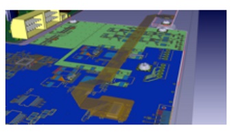
Zuken and Nano Dimension will share a booth and showcase the latest technologies for DFM and 3D printing. Zuken’s CR-8000 Design Force DfM software provides a platform to automate the process of applying the necessary rules for different board technologies, including flex, with the benefit of improving design quality and manufacturing yields. This software incorporates a database of design rules for many different manufacturing processes that take into account materials and technologies.
Nano Dimension will feature its DragonFly 2020 3D printer for professional electronics and nanotechnology-based conductive and dielectric materials for its 3D printers. DragonFly 2020 3D Printers enable companies involved in electronics to take control of their development cycles by 3D printing their own multi-layer PCB prototypes. The 3D printer continues to capture global industry and media attention.
Together, the companies’ combined offerings represent a complete solution for the design and manufacture of multi-layer PCBs unmatched in the industry. By using them together, development teams can introduce more agile development processes at every prototyping stage – from concept verification and design validation, to test fixtures. With these solutions, users can expect to spend more time innovating and getting new ideas to market, rather than dealing with design administration.
The two companies are presenting multiple sessions during the technical conference highlighting their technology expertise:
- Power Integrity and Decoupling Primer for PCB Designers
- Improve Flexible Printed Circuit Manufacturing Productivity with Better DfM Checks
- EDA Support and Roadmap for 3D Printing of PCBs
- 3D Printing: A New Dimension in Electronics Prototyping & Manufacturing
About Zuken
Zuken is a global provider of leading-edge software and consulting services for electrical and electronic design and manufacturing. Founded in 1976, Zuken has the longest track record of technological innovation and financial stability in the electronic design automation (EDA) software industry. The company’s extensive experience, technological expertise and agility, combine to create world-class software solutions. Zuken’s transparent working practices and integrity in all aspects of business produce long-lasting and successful customer partnerships that make Zuken a reliable long-term business partner.
Zuken is focused on being a long-term innovation and growth partner. The security of choosing Zuken is further reinforced by the company’s people—the foundation of Zuken’s success. Coming from a wide range of industry sectors, specializing in many different disciplines and advanced technologies, Zuken’s people relate to and understand each company’s unique requirements. For more information about the company and its products, click here.
About Nano Dimension Ltd.
Nano Dimension is a leading additive manufacturing technology company. Nano Dimension is disrupting, reshaping and defining the future of how electronics are made. With its unique 3D printing technologies, Nano Dimension is targeting the growing demand for electronic devices that require increasingly sophisticated features and rely on printed circuit boards (PCBs). Demand for circuitry, including PCBs -which are the heart of every electronic device - covers a diverse range of industries, including consumer electronics, medical devices, defense, aerospace, automotive, IoT and telecom. These sectors can all benefit greatly from Nano Dimension’s 3D printed electronics solutions for rapid prototyping and short-run manufacturing.
Share on:


Suggested Items
PCBA Market to Reach $147.5 Billion by 2035, Growing at a CAGR of 4.7% from 2025
06/27/2025 | PRNewswireThe Printed Circuit Board Assembly market is projected to reach $147.5 billion by 2035, up from an estimated $90.91 billion in 2025, growing at a steady CAGR of 4.7% during the forecast period.
Scanfil Strengthens its Customer Portfolio in Medtech & Life Science by Signing Agreement with Liquid Instruments
06/27/2025 | BUSINESS WIREScanfil and Liquid Instruments have signed a manufacturing outsourcing agreement for Scanfil’s Melbourne plant in Australia. This agreement supports Liquid Instruments’ strategy to onshore production of its flagship Moku platform, strengthening domestic supply chains and bringing manufacturing closer to its research and development hub.
Magnalytix and Foresite to Host Technical Webinar on SIR Testing and Functional Reliability
06/26/2025 | MAGNALYTIXMagnalytix, in collaboration with Foresite Inc., is pleased to announce an upcoming one-hour Webinar Workshop titled “Comparing SIR IPC B-52 to Umpire 41 Functional & SIR Test Method.” This session will be held on July 24, 2025, and is open to professionals in electronics manufacturing, reliability engineering, and process development seeking insights into new testing standards for climatic reliability.
Indium Corporation Expert to Present on Automotive and Industrial Solder Bonding Solutions at Global Electronics Association Workshop
06/26/2025 | IndiumIndium Corporation Principal Engineer, Advanced Materials, Andy Mackie, Ph.D., MSc, will deliver a technical presentation on innovative solder bonding solutions for automotive and industrial applications at the Global Electronics A
₹417 Crore Electronics Manufacturing Cluster Approved in Gautam Buddha Nagar, Uttar Pradesh
06/26/2025 | Government of India Press Information BureauGovernment of India approved the setting up of a ₹417 crore Electronics Manufacturing Cluster (EMC 2.0) at Gautam Buddha Nagar, Uttar Pradesh. It aims to boost local manufacturing and innovation.