


 The Right Approach: I Hear the Train A Comin'
 It’s Only Common Sense: OCCAM—the Time Is Now
 Marcy's Musings: The Growing Industry
Digging Sensors out of an Efficiency Hole
September 20, 2017 | A*STAREstimated reading time: 2 minutes
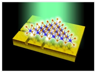
Future ultrathin solar cells and light sources could have their surfaces covered by tiny trenches, after A*STAR researchers found such structures enhance efficiency by four orders of magnitude.
Joel Yang from the A*STAR Institute of Materials Research and Engineering was part of an international collaboration that achieved a 20,000-fold increase in the photoluminescence of a one atom-thick layer of tungsten diselenide, by mounting it on a gold surface patterned with narrow trenches.
Tungsten diselenide is promising for ultra-sensitive, ultra-thin light sensors, solar cells and light-emitting diodes, because of its ability to absorb light and re-emit at a different frequency. However this effect only occurs for a single atom layer, so its efficiency is very low – most of the light passes straight through.
Yang’s inspiration was to mount the layer on a gold surface and trap the light energy at the interface of the two layers in the form of surface plasmons. To enhance the absorption of light, they added trenches to the gold layer under the tungsten diselenide.
“It was very surprising that such a large enhancement could be possible,” says Yang.
The key was matching the trench size to the energy so that the plasmons were trapped in the trenches through a resonant process known as the Purcell effect.
The team shone 633-nanometer light onto the sample and measured the output at 750 nanometers. They found 12 nm wide trenches in a grid pattern with spacing 200 nanometers gave the highest photoluminescence – 20,000 times more than a bare layer of tungsten diselenide.
To create the structure, the team etched a very flat silicon crystal to create a grid of ridges. Next they deposited a layer of gold onto the silicon and then peeled it off to reveal trenches where the ridges had been.
“The narrowness of the trenches and the flatness of the metal film is important,” Yang says. “Any roughness will interact detrimentally with the two-dimensional material.”
The gold was immersed in water and a film of tungsten diselenide floated on the water’s surface. The gold was then slowly raised out of the solution, emerging with the thin layer on top.
The simple structure has many advantages, says Yang. “The entire surface is exposed to the user, which makes it easy for further research, such as functionalizing the surface with chemicals or adding electrodes”.
It is also easier to manufacture than other plasmonic devices, which require a second layer above the thin layer, creating a sandwich.
Share on:


Suggested Items
Real Time with… IPC APEX EXPO 2024: Exploring the Future of Surface Finishes
04/25/2024 | Real Time with...IPC APEX EXPOJoe McGurran, product marketing director for MKS Atotech, looks into the future of surface finishes, discussing less nickel, reduced thickness, technologies influencing HDI and UHDI, and the benefits of nickel-free surface finishes. He also touches on popular finishes like ENIG and palladium immersion gold and discusses the value proposition of making a change.
Designer’s Notebook: What Designers Need to Know About Manufacturing, Part 2
04/24/2024 | Vern Solberg -- Column: Designer's NotebookThe printed circuit board (PCB) is the primary base element for providing the interconnect platform for mounting and electrically joining electronic components. When assessing PCB design complexity, first consider the component area and board area ratio. If the surface area for the component interface is restricted, it may justify adopting multilayer or multilayer sequential buildup (SBU) PCB fabrication to enable a more efficient sub-surface circuit interconnect.
IDTechEx Report Unveils 3D Electronics Status and Opportunities
04/22/2024 | PRNewswire3D electronics is an emerging manufacturing approach that enables electronics to be integrated within or onto the surface of objects. 3D electronic manufacturing techniques empower new features, including mass customizability, greater integration, and improved sustainability in the electronics industry.
NASA, Japan Advance Space Cooperation, Sign Agreement for Lunar Rover
04/11/2024 | NASANASA Administrator Bill Nelson and Japan’s Minister of Education, Culture, Sports, Science and Technology (MEXT) Masahito Moriyama have signed an agreement to advance sustainable human exploration of the Moon.
Lockheed Martin Conducts Historic LRASM Flight Test
04/04/2024 | Lockheed MartinThe U.S. Navy in partnership with Lockheed Martin [NYSE: LMT] successfully conducted a historic Long-Range Anti-Ship Missile (LRASM) flight test with four missiles simultaneously in flight.