


 The Right Approach: I Hear the Train A Comin'
 It’s Only Common Sense: OCCAM—the Time Is Now
 Marcy's Musings: The Growing Industry
A Little Tension Yields Enormous Solar Crystals
September 26, 2017 | KAUSTEstimated reading time: 2 minutes
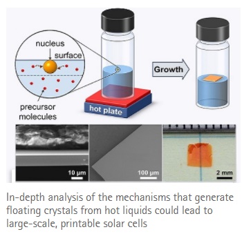
In the race to replace silicon in low-cost solar cells, semiconductors known as metal halide perovskites are favored because they can be solution-processed into thin films with excellent photovoltaic efficiency. A collaboration between KAUST and Oxford University researchers has now uncovered a strategy that grows perovskites into centimeter-scale, highly pure crystals thanks to the effect of surface tension.
In their natural state, perovskites have difficultly moving solar-generated electricity because they crystallize with randomly oriented grains. Osman Bakr from KAUST’s Solar Center and coworkers are working on ways to dramatically speed up the flow of these charge carriers using inverse temperature crystallization (ITC). This technique uses special organic liquids and thermal energy to force perovskites to solidify into structures resembling single crystals—the optimal arrangements for device purposes.
While ITC produces high-quality perovskites far faster than conventional chemical methods, the curious mechanisms that initiate crystallization in hot organic liquids are poorly understood. Ayan Zhumekenov, a PhD student in Bakr’s group, recalls spotting a key piece of evidence during efforts to adapt ITC toward large-scale manufacturing. “At some point, we realized that when crystals appeared, it was usually at the solution’s surface,” he says. “And this was particularly true when we used concentrated solutions.”
The KAUST team partnered with Oxford theoreticians to identify how interfaces influence perovskite growth in ITC. They propose that metal halides and solvent molecules initially cling together in tight complexes that begin to stretch and weaken at higher temperatures. With sufficient thermal energy, the complex breaks and perovskites begin to crystallize.
But interestingly, the researchers found that complexes located at the solution surface can experience additional forces due to surface tension—the strong cohesive forces that enable certain insects to stride over lakes and ponds. The extra pull provided by the surface makes it much easier to separate the solvent-perovskite complexes and nucleate crystals that float on top of the liquid.
Exploiting this knowledge helped the team produce centimeter-sized, ultrathin single crystals and prototype a photodetector with characteristics comparable to state-of-the-art devices. Although the single crystals are currently fragile and difficult to handle due to their microscale thicknesses, Zhumekenov explains that this method could help direct the perovskite growth onto specific substrates.
“Taking into account the roles of interfaces and surface tension could have a fundamental impact,” he says, “we can get large-area growth, and it’s not limited to specific metal cations—you could have a library of materials with perovskite structures.”
Share on:


Suggested Items
Real Time with… IPC APEX EXPO 2024: Exploring the Future of Surface Finishes
04/25/2024 | Real Time with...IPC APEX EXPOJoe McGurran, product marketing director for MKS Atotech, looks into the future of surface finishes, discussing less nickel, reduced thickness, technologies influencing HDI and UHDI, and the benefits of nickel-free surface finishes. He also touches on popular finishes like ENIG and palladium immersion gold and discusses the value proposition of making a change.
Designer’s Notebook: What Designers Need to Know About Manufacturing, Part 2
04/24/2024 | Vern Solberg -- Column: Designer's NotebookThe printed circuit board (PCB) is the primary base element for providing the interconnect platform for mounting and electrically joining electronic components. When assessing PCB design complexity, first consider the component area and board area ratio. If the surface area for the component interface is restricted, it may justify adopting multilayer or multilayer sequential buildup (SBU) PCB fabrication to enable a more efficient sub-surface circuit interconnect.
IDTechEx Report Unveils 3D Electronics Status and Opportunities
04/22/2024 | PRNewswire3D electronics is an emerging manufacturing approach that enables electronics to be integrated within or onto the surface of objects. 3D electronic manufacturing techniques empower new features, including mass customizability, greater integration, and improved sustainability in the electronics industry.
NASA, Japan Advance Space Cooperation, Sign Agreement for Lunar Rover
04/11/2024 | NASANASA Administrator Bill Nelson and Japan’s Minister of Education, Culture, Sports, Science and Technology (MEXT) Masahito Moriyama have signed an agreement to advance sustainable human exploration of the Moon.
Lockheed Martin Conducts Historic LRASM Flight Test
04/04/2024 | Lockheed MartinThe U.S. Navy in partnership with Lockheed Martin [NYSE: LMT] successfully conducted a historic Long-Range Anti-Ship Missile (LRASM) flight test with four missiles simultaneously in flight.