


 The Right Approach: I Hear the Train A Comin'
 It’s Only Common Sense: OCCAM—the Time Is Now
 Marcy's Musings: The Growing Industry
Liquid Metal Breakthrough Ushers New Wave of Electronics
October 25, 2017 | RMIT UniversityEstimated reading time: 2 minutes
RMIT researchers have used liquid metal to create two-dimensional materials no thicker than a few atoms that have never before been seen in nature.
The incredible breakthrough will not only revolutionise the way we do chemistry but could be applied to enhance data storage and make faster electronics. The “once-in-a-decade” discovery has been published in Science.
The researchers dissolve metals in liquid metal to create very thin oxide layers, which previously did not exist as layered structures and which are easily peeled away.
Once extracted, these oxide layers can be used as transistor components in modern electronics. The thinner the oxide layer, the faster the electronics are. Thinner oxide layers also mean the electronics need less power. Among other things, oxide layers are used to make the touch screens on smart phones.
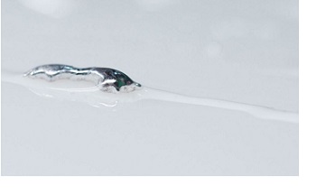
This image of a liquid metal "slug" and its clear atom-thick "trail" shows the breakthrough in action. When dissolved in a liquid metal core, certain metals leave behind this clear layer of their oxide, which is no thicker than a few atoms and can be peeled away by touching or rolling.
The research is led by Professor Kourosh Kalantar-zadeh and Dr Torben Daeneke from RMIT’s School of Engineering, who with students have been experimenting with the method for the last 18 months.
“When you write with a pencil, the graphite leaves very thin flakes called graphene, that can be easily extracted because they are naturally occurring layered structures,” said Daeneke. “But what happens if these materials don’t exist naturally?
“Here we found an extraordinary, yet very simple method to create atomically thin flakes of materials that don't naturally exist as layered structures.
“We use non-toxic alloys of gallium (a metal similar to aluminium) as a reaction medium. This covers the surface of the liquid metal with atomically thin oxide layers of the added metal rather than the naturally occurring gallium oxide.
“This oxide layer can then be exfoliated by simply touching the liquid metal with a smooth surface. Larger quantities of these atomically thin layers can be produced by injecting air into the liquid metal, in a process that is similar to frothing milk when making a cappuccino.”
It’s a process so cheap and simple that it could be done on a kitchen stove by a non-scientist.
“I could give these instructions to my mum, and she would be able to do this at home,” Daeneke said.
Professor Kourosh Kalantar-zadeh said that the discovery now places previously unseen thin oxide materials into everyday reach, with profound implications for future technologies.
“We predict that the developed technology applies to approximately one-third of the periodic table. Many of these atomically thin oxides are semiconducting or dielectric materials.
“Semiconducting and dielectric components are the foundation of today’s electronic and optical devices. Working with atomically thin components is expected to lead to better, more energy efficient electronics. This technological capability has never been accessible before.”
The breakthrough could also be applied to catalysis, the basis of the modern chemical industry, reshaping how we make all chemical products including medicines, fertilisers and plastics.
The research is funded by the Australian Research Council Centre for Future Low-Energy Electronics Technologies (FLEET).
Share on:


Suggested Items
Warm Windows and Streamlined Skin Patches – IDTechEx Explores Flexible and Printed Electronics
04/26/2024 | IDTechExFlexible and printed electronics can be integrated into cars and homes to create modern aesthetics that are beneficial and easy to use. From luminous car controls to food labels that communicate the quality of food, the uses of this technology are endless and can upgrade many areas of everyday life.
Book Excerpt: The Printed Circuit Assembler’s Guide to... Factory Analytics
04/24/2024 | I-Connect007 Editorial TeamIn our fast-changing, deeply competitive, and margin-tight industry, factory analytics can be the key to unlocking untapped improvements to guarantee a thriving business. On top of that, electronics manufacturers are facing a tremendous burden to do more with less. If you don't already have a copy of this book, what follows is an excerpt from the introduction chapter of 'The Printed Circuit Assembler’s Guide to... Factory Analytics: Unlocking Efficiency Through Data Insights' to whet your appetite.
Listen Up! The Intricacies of PCB Drilling Detailed in New Podcast Episode
04/25/2024 | I-Connect007In episode 5 of the podcast series, On the Line With: Designing for Reality, Nolan Johnson and Matt Stevenson continue down the manufacturing process, this time focusing on the post-lamination drilling process for PCBs. Matt and Nolan delve into the intricacies of the PCB drilling process, highlighting the importance of hole quality, drill parameters, and design optimization to ensure smooth manufacturing. The conversation covers topics such as drill bit sizes, aspect ratios, vias, challenges in drilling, and ways to enhance efficiency in the drilling department.
Elevating PCB Design Engineering With IPC Programs
04/24/2024 | Cory Blaylock, IPCIn a monumental stride for the electronics manufacturing industry, IPC has successfully championed the recognition of the PCB Design Engineer as an official occupation by the U.S. Department of Labor (DOL). This pivotal achievement not only underscores the critical role of PCB design engineers within the technology landscape, but also marks the beginning of a transformative journey toward nurturing a robust, skilled workforce ready to propel our industry into the future.
Winner of The Science Show Rakett 69 Receives Incap Scholarship
04/24/2024 | IncapThe winner of the Rakett 69 science show, Andri Türkson, who stood out as an electronics enthusiast, received a scholarship from Incap Estonia, along with an internship opportunity in Saaremaa.