


 The Right Approach: I Hear the Train A Comin'
 It’s Only Common Sense: OCCAM—the Time Is Now
 Marcy's Musings: The Growing Industry
New Motion Sensors a Major Step Toward Low-Cost, High-Performance Wearable Technology
November 17, 2017 | Florida State UniversityEstimated reading time: 3 minutes
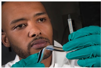
Researchers from the FAMU-FSU College of Engineering have developed a class of breakthrough motion sensors that could herald a near future of ubiquitous, fully integrated and affordable wearable technology.
In a paper published in the journal Materials and Design, engineers from FSU’s High-Performance Materials Institute, in collaboration with scientists from Institut National des Sciences Appliquées in Lyon, France, detail the impressive properties and cost-effective manufacturing process of an advanced series of motion sensors made using buckypaper — razor thin, flexible sheets of pure, exceptionally durable carbon nanotubes.
These new buckypaper sensors represent a marked improvement on current industry standards, with most sensors being either too crude or too inflexible to reliably monitor complex structures like the human body.
“Current technology is not designed for that,” said Richard Liang, director of the High-Performance Materials Institute and professor at the FAMU-FSU College of Engineering. “For sensor technology, you need it to be flexible, you need it to be affordable and you need it to be scalable. This new technology is versatile and the sensors are affordable to print. It’s a big innovation that presents many possibilities down the road.”
At this stage, potential applications for the printable buckypaper sensors are limited only by the breadth of researchers’ imaginations. The low-profile design could be integrated into bedsheets to monitor quality of sleep, shoes to track step count and posture or workout clothes to measure intensity of exercise.
Researchers also foresee potential applications beyond the realm of wearable technology. In the field of soft robotics, the material could facilitate advances in the production of responsive, self-correcting artificial muscles.
Moreover, the scalable sensors represent another step toward the long-predicted future of an “internet of things,” where virtually all of an individual’s computers, devices, garments, furniture and appliances are digitally connected to freely exchange information in the cloud.
“Most projects don’t have this many possible applications,” said doctoral candidate Joshua DeGraff, the lead author of the study. “This material could be used in structural health monitoring, wearable technology and everything in between. I’m excited because this is something that can affect a lot of people in their everyday lives.”
The novel sensor structure combines a strip of seven micron-thin buckypaper with silver ink electrodes printed from a common, commercially available ink-jet printer.
The result is a kind of perfect Goldilocks sensor: not as insensitive as common, flexible metallic sensors, but not as rigid or cumbersome as popular, more sensitive semi-conductor sensors.
The wearable buckypaper sensors are an ideal marriage of these competing qualities. They’re flexible, seamless and sensitive to subtle movements and strains.
“We measure sensors by gauge factor, which indicates how much resistance value changes as a material is strained or bent,” DeGraff said. “Our gauge factor has been up to eight times higher than commercial sensors and 75 percent higher than many other carbon nanotube sensors.”
As development of the printable sensor technology continues, researchers hope to improve upon the already remarkable thinness of the material so that it can be integrated into comfortable and non restrictive clothing. Additional testing on complex model structures is required to ensure the material’s ability to conform to the variable curves and crevices of the human body.
While the technology might not be ready for primetime quite yet, researchers are energized by its promising future.
“As engineering professors, we want to see the things we create in the lab become successful products,” Liang said. “We’re not quite there yet, but this is an important step. Consumers want great quality and affordable prices, and this material provides both of those things.”
The research was supported by the Florida Education Fund’s McKnight Doctoral Fellowship program, the National Science Foundation Scalable Nanomanufacturing Program and the Région Auvergne Rhône-Alpes “CMIRA Accueil Doc” fellowship program.
Share on:


Suggested Items
Warm Windows and Streamlined Skin Patches – IDTechEx Explores Flexible and Printed Electronics
04/26/2024 | IDTechExFlexible and printed electronics can be integrated into cars and homes to create modern aesthetics that are beneficial and easy to use. From luminous car controls to food labels that communicate the quality of food, the uses of this technology are endless and can upgrade many areas of everyday life.
iNEMI Packaging Tech Topic Series: Role of EDA in Advanced Semiconductor Packaging
04/26/2024 | iNEMIAdvanced semiconductor packaging with heterogenous integration has made on-package integration of multiple chips a crucial part of finding alternatives to transistor scaling. Historically, EDA tools for front-end and back-end design have evolved separately; however, design complexity and the increased number of die-to-die or die-to-substrate interconnections has led to the need for EDA tools that can support integration of overall design planning, implementation, and system analysis in a single cockpit.
Koh Young Showcases Award-winning Inspection Solutions at SMTconnect with SmartRep in Hall 4A.225
04/25/2024 | Koh Young TechnologyKoh Young Technology, the industry leader in True 3D measurement-based inspection solutions, will showcase an array of award-winning inspection and measurement solutions at SMTconnect alongside its sales partner, SmartRep, in booth 4A.225 at NürnbergMesse from June 11-13, 2023. The following offers a glimpse into what Koh Young will present at the tradeshow:
Real Time with… IPC APEX EXPO 2024: Plasmatreat: Innovative Surface Preparation Solutions
04/25/2024 | Real Time with...IPC APEX EXPOIn this interview, Editor Nolan Johnson speaks with Hardev Grewal, CEO and president of Plasmatreat, a developer of atmospheric plasma solutions. Plasmatreat uses clean compressed air and electricity to create plasma, offering environmentally friendly methods for surface preparation. Their technology measures plasma density for process optimization and can remove organic micro-contamination. Nolan and Hardev also discuss REDOX-Tool, a new technology for removing metal oxides.
Nanotechnology Market to Surpass $53.51 Billion by 2031
04/25/2024 | PRNewswireSkyQuest projects that the nanotechnology market will attain a value of USD 53.51 billion by 2031, with a CAGR of 36.4% over the forecast period (2024-2031).