


 The Right Approach: I Hear the Train A Comin'
 It’s Only Common Sense: OCCAM—the Time Is Now
 Marcy's Musings: The Growing Industry
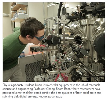
'Magnetoelectric' Material Shows Promise as Memory for Electronics
November 30, 2017 | University of Wisconsin-MadisonEstimated reading time: 2 minutes
Smartphones and computers wouldn’t be nearly as useful without room for lots of apps, music and videos.
Devices tend to store that information in two ways: through electric fields (think of a flash drive) or through magnetic fields (like a computer’s spinning hard disk). Each method has advantages and disadvantages. However, in the future, our electronics could benefit from the best of each.
“There’s an interesting concept,” says Chang-Beom Eom, the Theodore H. Geballe Professor and Harvey D. Spangler Distinguished Professor of Materials Science and Engineering at the University of Wisconsin–Madison. “Can you cross-couple these two different ways to store information? Could we use an electric field to change the magnetic properties? Then you can have a low-power, multifunctional device. We call this a ‘magnetoelectric’ device.”
In research published recently in the journal Nature Communications, Eom and his collaborators describe not only their unique process for making a high-quality magnetoelectric material, but exactly how and why it works.
Magnetoelectric materials — which have both magnetic and electrical functionalities, or “orders” — already exist. Switching one functionality induces a change in the other.
“It’s called cross-coupling,” says Eom. “Yet, how they cross-couple is not clearly understood.”
Gaining that understanding, he says, requires studying how the magnetic properties change when an electric field is applied. Up to now, this has been difficult due to the complicated structure of most magnetoelectric materials.
In the past, says Eom, people studied magnetoelectric properties using very “complex” materials, or those that lack uniformity. In his approach, Eom simplified not only the research, but the material itself.
Drawing on his expertise in material growth, he developed a unique process, using atomic “steps,” to guide the growth of a homogenous, single-crystal thin film of bismuth ferrite. Atop that, he added cobalt, which is magnetic; on the bottom, he placed an electrode made of strontium ruthenate.
The bismuth ferrite material was important because it made it much easier for Eom to study the fundamental magnetoelectric cross-coupling.
“We found that in our work, because of our single domain, we could actually see what was going on using multiple probing, or imaging, techniques,” he says. “The mechanism is intrinsic. It’s reproducible — and that means you can make a device without any degradation, in a predictable way.”
To image the changing electric and magnetic properties switching in real time, Eom and his colleagues used the powerful synchrotron light sources at Argonne National Laboratory outside Chicago, and in Switzerland and the United Kingdom.
“When you switch it, the electrical field switches the electric polarization. If it’s ‘downward,’ it switches ‘upward,’” he says. “The coupling to the magnetic layer then changes its properties: a magnetoelectric storage device.”
That change in direction enables researchers to take the next steps needed to add programmable integrated circuits — the building blocks that are the foundation of our electronics — to the material.
While the homogenous material enabled Eom to answer important scientific questions about how magnetoelectric cross-coupling happens, it also could enable manufacturers to improve their electronics.
“Now we can design a much more effective, efficient and low-power device,” he says.
Eom’s team includes both theorists and experimentalists, including UW–Madison physics Professor Mark Rzchowski and collaborators at Diamond Light Source in England, Temple University, the University of Oxford, Argonne National Laboratory, Swiss Light Source, Luxembourg Institute of Science and Technology, and Northern Illinois University.
Share on:


Suggested Items
Inkjet Solder Mask ‘Has Arrived’
04/10/2024 | Pete Starkey, I-Connect007I was delighted to be invited to attend an interactive webinar entitled “Solder Mask Coating Made Easy with Additive Manufacturing,” hosted by SUSS MicroTec Netherlands in Eindhoven. The webinar was introduced and moderated by André Bodegom, managing director at Adeon Technologies, and the speakers were Mariana Van Dam, senior product manager PCB imaging solutions at AGFA in Belgium; Ashley Steers, sales manager at Electra Polymers in the UK; and Dr. Luca Gautero, product manager at SUSS MicroTec Netherlands.
NetVia Group Acquires Direct Imaging from Mivatek
04/09/2024 | Miva TechnologiesMiva Technologies is pleased to announce NetVia Group, Irving, TX has acquired a new Miva 2400NG Dual Tray Direct Imaging System with 30-micron capabilities for inner, outer and soldermask imaging.
Teledyne to Acquire Adimec
02/13/2024 | TeledyneTeledyne Technologies Incorporated announced that it has entered into an agreement to acquire Adimec Holding B.V. and its subsidiaries.
Real Time with... productronica 2023: MivaTek Global Advances Technology With High-res Imaging System
12/08/2023 | Real Time with...productronicaMivaTek's Brendan Hogan talks about how the company employs Digitally Adaptive Rasterization Technology (DART) in their high-res imaging equipment. He also shares how the blurred line between semiconductors and microelectronics is driving broader application of the imaging process.
Keysight Enables Validation of Arbe 4D Imaging Radar Chipset
11/30/2023 | Keysight Technologies, Inc.Keysight Technologies, Inc. announces that Arbe has selected the E8719A Radar Target Solution (RTS) to test the Arbe 4D imaging radar chipset for automotive applications.