


 It’s Only Common Sense: Nice Guys Really Can Finish First
 The Right Approach: I Hear the Train A Comin'
 Marcy's Musings: The Growing Industry
Study Reveals Secrets of ‘Fluid-Like’ Heat Flow in Solid Semiconductor at Nanoscale
January 18, 2018 | Purdue UniversityEstimated reading time: 3 minutes
Researchers are applying the same “hydrodynamic transport model” used to study flow in fluids to explain heat transport in a solid semiconductor, with potential implications for the design of high-speed transistors and lasers.
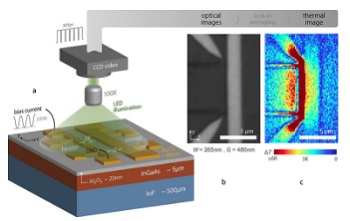
Image caption: Purdue University researchers have visualized temperature changes produced by ultra-small heat sources, gold strips formed on top of the semiconductor indium gallium arsenide. The work has potential implications for the design of high-speed transistors and lasers. This image (a) depicts the device structure and experimental setup, an optical image (b) of the fabricated device and (c) an experimental thermal image. (Purdue University image/Amirkoushyar Ziabari, Bjorn Vermeersch)
Thermal imaging of tiny nanoscale semiconductor heat sources revealed details about vortices of heat-carrying objects called phonons.
The new findings have potentially important implications for “thermal crosstalk,” in which multiple heat sources next to each other impact the overall temperature of the system, hindering performance. The researchers used a technique called full-field thermoreflectance thermal imaging to directly visualize temperature changes produced by ultra-small heat sources, gold strips formed on top of the semiconductor indium gallium arsenide.
The research concerns the crucial role of phonons, quantum-mechanical objects, or “quasiparticles,” that describe how vibrations travel through a material's crystal structure. The phonons are said to be “heat carriers” in solid materials.
“This is the first time such hydrodynamic effects are indirectly observed for heat propagation in a solid,” said Ali Shakouri, Purdue University's Mary Jo and Robert L. Kirk Director of the Birck Nanotechnology Center and a professor of electrical and computer engineering. “While structures called vortices are common in fluid flows such as water or air, this is the first time we’ve seen that they can be present inside solids for phonon flow in the typical semiconductor indium gallium arsenide, which is used in high-speed transistors and lasers.”
“The observed thermal crosstalk reduction has important implications in the design of nanoscale electronic and optoelectronic devices,” said Purdue postdoctoral research associate Amirkoushyar Ziabari, the paper’s lead author. “As the size of electronic and optoelectronic devices are getting smaller, there are more and more devices being packed into a smaller area, so the thermal crosstalk between these devices becomes important. Knowing the accurate thermal behavior in the neighborhood and a few microns from heat sources would help design better state-of-the-art devices in terms of performance, speed, thermal reliability, and so on.”
The researchers found that the reduced thermal crosstalk is caused by vortices generated near the edge of the heat sources.
“This is similar to the vortices that are observed at the edge of an obstacle placed inside of a current of air or water, such as behind an airplane wing,” Shakouri said.
The governing law of heat conduction, known as the Fourier Law or the heat-diffusion equation, does not accurately predict thermal transport for devices on the nanoscale. Because the Fourier diffusion equation doesn't explain the heat transport at those scales, this transport regime is called non-diffusive.
“As the size of electronic and optoelectronic devices are getting smaller, it is important to consider this non-diffusive behavior for design and optimization of such small devices,” Ziabari said. “These new measurements show that at nanoscales, heat propagation has interesting ‘fluid-like’ behavior.”
Conventional methods do not account for vortices of heat transport found at the nanoscale.
“Vorticity only becomes important when the characteristic source dimension is comparable to the hydrodynamic length scale of about 150 nanometers,” he said.
The Fourier theory substantially overestimates the experimentally observed temperature a short distance away from the heater lines.
“The surprising effect was that the temperature decays much faster than what Fourier theory predicted,” Shakouri said. “Within a distance of 1 or 2 microns of a small heat source - a line about 100 nanometers wide - temperature could be one-third to one-fourth what Fourier theory predicts.”
The thermoreflectance thermal imaging approach allows researchers to create maps of temperature rise at far higher resolution than otherwise possible using light in the visible range.
Share on:


Suggested Items
Real Time with… IPC APEX EXPO 2024: Ventec Discusses New Pro-bond Family of Advanced Products
05/01/2024 | Real Time with...IPC APEX EXPOChris Hanson, Ventec's Global Head of IMS Technology, outlines the launch of four pro-bond formulas that deliver an outstanding combination of low dissipation factor (Df) with a dielectric constant (Dk) range to maximize the design window for critical PCB parameters. As Chris points out, Pro-bond is designed for low-loss, high-speed applications, while thermal-bond dissipates heat from a component through the board to a heat sink.
IPC's Vision for Empowering PCB Design Engineers
04/30/2024 | Robert Erickson, IPCAs architects of innovation, printed circuit board designers are tasked with translating increasingly complex concepts into tangible designs that power our modern world. IPC provides the necessary community, standards framework, and education to prepare these pioneers as they explore the boundaries of what’s possible, equipping engineers with the knowledge, skills, and resources required to thrive in an increasingly dynamic field.
iNEMI Packaging Tech Topic Series: Role of EDA in Advanced Semiconductor Packaging
04/26/2024 | iNEMIAdvanced semiconductor packaging with heterogenous integration has made on-package integration of multiple chips a crucial part of finding alternatives to transistor scaling. Historically, EDA tools for front-end and back-end design have evolved separately; however, design complexity and the increased number of die-to-die or die-to-substrate interconnections has led to the need for EDA tools that can support integration of overall design planning, implementation, and system analysis in a single cockpit.
Cadence, TSMC Collaborate on Wide-Ranging Innovations to Transform System and Semiconductor Design
04/25/2024 | Cadence Design SystemsCadence Design Systems, Inc. and TSMC have extended their longstanding collaboration by announcing a broad range of innovative technology advancements to accelerate design, including developments ranging from 3D-IC and advanced process nodes to design IP and photonics.
Ansys, TSMC Enable a Multiphysics Platform for Optics and Photonics, Addressing Needs of AI, HPC Silicon Systems
04/25/2024 | PRNewswireAnsys announced a collaboration with TSMC on multiphysics software for TSMC's Compact Universal Photonic Engines (COUPE). COUPE is a cutting-edge Silicon Photonics (SiPh) integration system and Co-Packaged Optics platform that mitigates coupling loss while significantly accelerating chip-to-chip and machine-to-machine communication.